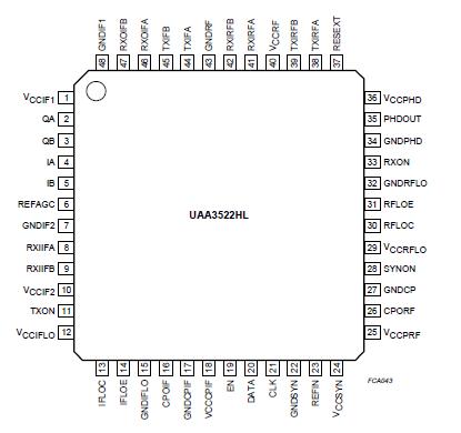
Features: · Dual-band application for Global System for Mobile communication (GSM) and Digital Cellularcommunication Systems (DCS)· Low noise and wide dynamic range single Intermediate Frequency (IF) transceiver· More than 30 dB on-chip image rejection in the receiver· More than 60 dB gain control...
UAA3522HL: Features: · Dual-band application for Global System for Mobile communication (GSM) and Digital Cellularcommunication Systems (DCS)· Low noise and wide dynamic range single Intermediate Frequency (IF...
SeekIC Buyer Protection PLUS - newly updated for 2013!
268 Transactions
All payment methods are secure and covered by SeekIC Buyer Protection PLUS.
SYMBOL |
PARAMETER |
MIN. |
TYP. |
MAX. |
UNIT |
VCCn |
supply voltage |
-0.3 |
- |
+6 |
V |
Ptot |
total power dissipation |
- |
- |
1 |
W |
Tstg |
storage temperature |
-40 |
- |
+150 |
°C |
Tamb |
ambient temperature |
-30 |
- |
+70 |
°C |
The UAA3522HL integrates the receiver and most of the transmitter section of a GSM hand-held transceiver. It also integrates the receiver IF and the transmitter section of a DCS transceiver.
The receiver comprises an RF and an IF section. The RF (GSM) front-end amplifies the aerial signal, converts the chosen channel frequency to an IF of 200 MHz, and UAA3522HL also provides more than 30 dB of image suppression. Some selectivity is provided at this stage by an off-chip bandpass pre-filter. The IF section further amplifies the chosen channel, maintains the gain at the required level,demodulates the signal into I and Q components, and provides channel selectivity at a baseband stage using a high performance integrated low-pass filter. The IF gain can be varied over a range of more than 60 dB. The offset at the I and Q outputs of UAA3522HL can be cancelled out by software using the 3-wire serial programming bus.
The input Low Noise Amplifier (LNA)UAA3522HL can be switched off via the bus to allow accurate calibration in the offset
cancellation mode.
The transmitter UAA3522HL comprises a high precision I/Q modulator and modulation loop architecture. The I/Q modulator converts the baseband modulation frequency to the transmit IF. The modulation loop architecture, which includes an on-chip offset mixer and phase detector,controls an external transmit RF VCO which converts the transmit modulated IF signal to RF.
A receive RF VCO provides the Local Oscillator (LO) signal to the image rejection mixers in the RF receiver. An IF VCO provides the LO signal to the I/Q demodulator and I/Q modulator in the receiver and transmitter sections respectively.
The frequencies of the RF VCO and the IF VCO are set by internal PLL circuits, which are programmable via the 3-wire serial bus. The RF and IF PLL UAA3522HL comparison frequencies are 200 kHz and 1 MHz respectively, derived from a 13 MHz reference signal which has to be supplied externally. The quadrature RF LO signals required by the image rejection mixers are obtained using on-chip Resistor Capacitor (RC) networks. The quadrature IF LO signals required by the I/Q modulator and I/Q demodulator are obtained by dividing the frequency of the IF VCO signal.
The UAA3522HL can be powered on in either receiver (RX),transmitter (TX) or synthesizer (SYN) operating mode depending on the logic level at pins RXON, TXON and SYNON, respectively. Alternatively, an operating mode of UAA3522HL can be selected by software using the 3-wire serial programming bus. In RX or TX mode, only those sections of the IC which are required are switched on.
The GSM or DCS band is selected by the 3-wire serial programming bus. When activating RX mode for DCS applications, the receiver RF section UAA3522HL can be disabled by software so that only the receiver IF section is powered-on.
The SYN mode is used to power-on the synthesizer prior to activating the RX or TX mode. In SYN mode, some internal LO buffers are also powered-on to minimize the 'pulling' effect of the VCO when either the receiver or the transmitter are switched on.