Features: · Dual postamplifier
· Single 3.3 V power supply
· Wideband operation from 50 kHz to 2.5 GHz (typical value)
· Fully differential
· Channels are delay matched
· On-chip DC-offset compensations without external capacitor
· Interfacing with positive or negative supplied logic
· Switching possibility between channels
· Positive Emitter Coupled Logic (PECL) or Current-Mode Logic (CML) compatible data outputs adjustable from 200 to 800 mV (p-p) single-ended
· Power-down capability for unused outputs and detectors
· Rise and fall times 80 ps (typical value)
· Possibility to invert the output of each channel separately
· Input level-detection circuits for Received Signal Strength Indicator (RSSI) or Loss Of Signal (LOS) detection, programmable from 0.4 to 400 mV (p-p) single-ended, with open-drain comparator output for direct interfacing with positive or negative logic
· Reference voltage for output level and LOS adjustment
· Automatic strongest input signal switch possibility (TZA3019 version B)
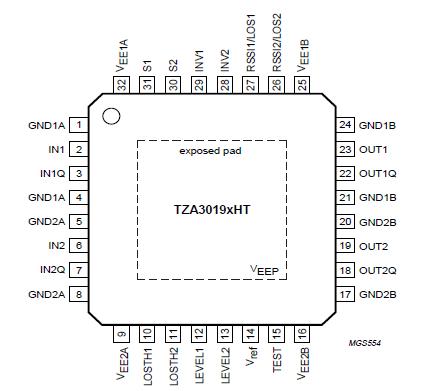
· HTQFP32 or HBCC32 plastic package with exposed pad.
Application· Postamplifier for Synchronous Digital Hierarchy and Synchronous Optical Network (SDH/SONET) transponder
· SDH/SONET wavelength converter
· Crosspoint or channel switch
· PECL driver
· Fibre channel arbitrated loop
· Protection ring
· Monitoring
· Signal level detectors
· Swing converter CML 200 mV (p-p) to PECL 800 mV (p-p)
· Port bypass circuit
· 2.5 GHz clock amplification.Pinout Specifications
|
SYMBOL |
PARAMETER |
MIN. |
MAX. |
UNIT |
| VEE |
negative supply voltage |
-5.5 |
+0.5 |
V |
| Vn |
DC voltage
pins IN1, IN1Q, IN2, IN2Q, LOSTH1, LOSTH2, LEVEL1, LEVEL2,
Vref, TEST, OUT2Q, OUT2, OUT1Q, OUT1, VEEP, GND1A,
GND2A, GND1B and GND2B
pins LOS1, LOS2, INV1, INV2, S1 and S2 |
VEE - 0.5
VEE - 0.5 |
0.5
VEE + 7 |
V
V |
| In |
DC current
pins IN1, IN1Q, IN2 and IN2Q
pins LOSTH1, LOSTH2, LEVEL1 and LEVEL2
pins Vref, TEST, LOS1 and LOS2
pins OUT1, OUT1Q, OUT2 and OUT2Q
pins INV1, INV2, S1 and S2 |
-20
0
-1
-30
0 |
+20
14
+1
+30
20
|
mA
A
mA
mA
A |
| Ptot |
total power dissipation |
- |
1.2 |
W |
| Tstg |
storage temperature |
-65 |
+150 |
°C |
| Tj |
junction temperature |
- |
150 |
°C |
| Tamb |
ambient temperature |
-40 |
+85 |
°C |
DescriptionThe TZA3019 is a low gain postamplifier multiplexer with a dual RSSI and/or LOS detector that is designed for use in critical signal path control applications, such as loop-through, redundant channel switching or Wavelength Division Multiplexing (WDM). The signal path is unregistered, so no clock is required for the data inputs.The signal path is fully differential and delay matched. It is capable of operating from 50 kHz to 2.5 GHz.
The TZA3019 HTQFP32 and HBCC32 packages can be delivered in three versions:
· TZA3019AHT and TZA3019AV with two RSSI signals
· TZA3019BHT and TZA3019BV with one RSSI and one LOS signal
· TZA3019CHT and TZA3019CV with two LOS signals.

 TZA3019 Data Sheet


