TZA3015HW

Features: General` A-rabitteTM(1): supports any bit rate from 30 Mbit/s to 3.2 Gbit/s with one single reference frequency` 4-bit parallel interface` Selectable Double Data Rate (DDR, half clock rate) or Single Data Rate (SDR) clocking scheme on parallel interface, enabling easy interfacing with FP...

product image

TZA3015HW Picture
SeekIC No. : 004534342 Detail

TZA3015HW: Features: General` A-rabitteTM(1): supports any bit rate from 30 Mbit/s to 3.2 Gbit/s with one single reference frequency` 4-bit parallel interface` Selectable Double Data Rate (DDR, half clock rate...

floor Price/Ceiling Price

Part Number:
TZA3015HW
Supply Ability:
5000

Price Break

  • Qty
  • 1~5000
  • Unit Price
  • Negotiable
  • Processing time
  • 15 Days
Total Cost: $ 0.00

SeekIC Buyer Protection PLUS - newly updated for 2013!

  • Escrow Protection.
  • Guaranteed refunds.
  • Secure payments.
  • Learn more >>

Month Sales

268 Transactions

Rating

evaluate  (4.8 stars)

Upload time: 2025/1/11

Payment Methods

All payment methods are secure and covered by SeekIC Buyer Protection PLUS.

Notice: When you place an order, your payment is made to SeekIC and not to your seller. SeekIC only pays the seller after confirming you have received your order. We will also never share your payment details with your seller.
Product Details

Description


Features:

General
` A-rabitteTM(1): supports any bit rate from 30 Mbit/s to 3.2 Gbit/s with one single reference frequency
` 4-bit parallel interface
` Selectable Double Data Rate (DDR, half clock rate) or Single Data Rate (SDR) clocking scheme on parallel interface, enabling easy interfacing with FPGA devices
` I2C-bus and pin programmable
` Six selectable reference frequency ranges
` Transmitter, receiver and transceiver modes
` Clean-up loop back mode
` Line loop back mode
` Diagnostic loop back mode
` Serial loop timing mode
` Single 3.3 V power supply.

Limiter
` Limiting amplifier with typical 5 mV input sensitivity
` Received Signal Strength Indicator (RSSI)
` Loss Of Signal (LOS) indicator with adjustable threshold
` Differential overvoltage protection.

Data and clock recovery and synthesizer
` Supports any bit rate from 30 Mbit/s to 3.2 Gbit/s when using I2C-bus interface
` Supports eight pre-programmed (pin selectable) bit rates:
  SDH/SONET rates at 155.52 Mbit/s, 622.08 Mbit/s,2488.32 Mbit/s and 2666.06 Mbit/s (STM16/OC48 + FEC)
  Gigabit Ethernet at 1250 Mbit/s and 3125 Mbit/s
  Fibre Channel at 1062.5 Mbit/s and 2125 Mbit/s.
` Provides stable clock signal at LOS
` Frequency lock indicator for DCR
` Loss Of Lock (LOL) indicator for synthesizer
` ITU-T compliant jitter tolerance for Data and Clock Recovery (DCR)
` ITU-T compliant jitter transfer for DCR in clean-up loop back mode
` ITU-T compliant jitter generation for synthesizer.

Multiplexer
` 4 : 1 multiplexing ratio
` Supports co-directional and contra-directional clocking
` 4-stage FIFO for wide tolerance to clock skew
` Rail-to-rail parallel inputs compliant with LVPECL,Current-Mode Logic (CML) and LVDS
` Programmable parity checking
` CML data and clock outputs.

Demultiplexer
` 1 : 4 demultiplexing ratio
` Adjustable LVDS output swing
` Frame detection for SDH/SONET and Gigabit Ethernet (GE) frames.


I2C-bus configurable options
` Programmable frequency resolution of 10 Hz
` Independent receive and transmit bit rate
` Slice level adjustment to improve Bit Error Rate (BER)
` Six reference frequency ranges
` Adjustable swing for CML serial data and clock outputs
` Programmable polarity of RF I/Os
` Clock versus data swap for optimum connectivity
` Swap of parallel bus for optimum connectivity
` Mute function for a forced logic 0 output state
` Programmable parity
` Programmable 32-bit frame detection.


Application

· Any optical transmission system with line rates between 30 Mbit/s and 3.2 Gbit/s
· Physical interface IC in receive and transmit channels
· Transponder applications
· Dense wavelength division multiplexing systems
· Due to DDR clocking option, the ultimate physical interface for FPGA based designs.


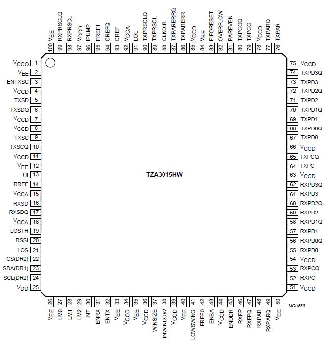
Pinout

  Connection Diagram


Specifications

SYMBOL
PARAMETER
MIN.
MAX.
UNIT
VCC analog supply voltage -0.5 +3.6 V
VDD digital supply voltage -0.5 +3.6 V
Vn DC voltage
on pins RXPC(Q), RXPD0(Q) to RXPD3(Q), RXFP(Q),
RXPAR(Q), TXPARERR(Q), TXPCO(Q), RXPRSCL(Q)and
TXPRSCL(Q)
on pins RXSD(Q), CREF(Q), TXPC(Q), TXPD0(Q) to TXPD3(Q),
TXPAR(Q), UI, RREF, LOSTH, RSSI, LOS, CS, SDA, SCL, LM0
to LM2, INT, ENRX, ENTX, WINSIZE, INWINDOW, ENDDR,
LOWSWING, ENBA, PAREVEN, OVERFLOW, FIFORESET,
ENTXSC, TXSD(Q), TXSC(Q), LOL, FREF0, FREF1, CLKDIR
and IPUMP
0.5


-0.5
VCC + 0.5


VCC + 0.5
V


V
In input current
on pins RXPC(Q), RXPD0(Q) to RXPD3(Q), RXFP(Q),
RXPAR(Q), TXPARERR(Q), TXPCO(Q), RXPRSCL(Q) and
TXPRSCL(Q)
on pins RXSD(Q) and CREF(Q)
on pin INT
on pins TXPC(Q), TXPD0(Q) to TXPD3(Q) and TXPAR(Q)

-20


-30
-2
-25


+20


+30
+2
+25


mA


mA
mA
mA

Tamb ambient temperature -40 +85 °C
Tj junction temperature - 125 °C
Tstg storage temperature -65 +150 °C


Description

The TZA3015HW is a fully integrated optical network transceiver containing a limiter, data and clock recovery circuit, clock synthesizer, 1 : 4 demultiplexer and 4 : 1 multiplexer.

The A-rate feature allows the IC to operate at any bit rate between 30 Mbit/s and 3.2 Gbit/s with one single reference frequency.
All clock signals of TZA3015HW are generated using a fractional N synthesizer with 10 Hz resolution offering a true continuous rate operating. For full configuration flexibility the transceiver can be programmed by pin and via the I2C-bus.


Customers Who Bought This Item Also Bought

Margin,quality,low-cost products with low minimum orders. Secure your online payments with SeekIC Buyer Protection.
LED Products
Power Supplies - External/Internal (Off-Board)
Optical Inspection Equipment
Optoelectronics
View more