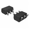
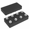
TXB0108

Features: ` 1.2 V to 3.6 V on A Port and 1.65 to 5.5 V on B Port (VCCA VCCB)` VCC Isolation Feature If Either VCC Input Is at GND, All Outputs Are in the High-Impedance State` OE Input Circuit Referenced to VCCA` Low Power Consumption, 4-mA Max ICC` Ioff Supports Partial-Power-Down Mode Operatio...

product image

TXB0108 Picture
SeekIC No. : 004534126 Detail

TXB0108: Features: ` 1.2 V to 3.6 V on A Port and 1.65 to 5.5 V on B Port (VCCA VCCB)` VCC Isolation Feature If Either VCC Input Is at GND, All Outputs Are in the High-Impedance State` OE Input Circuit Ref...

floor Price/Ceiling Price

Part Number:
TXB0108
Supply Ability:
5000

Price Break

  • Qty
  • 1~5000
  • Unit Price
  • Negotiable
  • Processing time
  • 15 Days
Total Cost: $ 0.00

SeekIC Buyer Protection PLUS - newly updated for 2013!

  • Escrow Protection.
  • Guaranteed refunds.
  • Secure payments.
  • Learn more >>

Month Sales

268 Transactions

Rating

evaluate  (4.8 stars)

Upload time: 2024/11/22

Payment Methods

All payment methods are secure and covered by SeekIC Buyer Protection PLUS.

Notice: When you place an order, your payment is made to SeekIC and not to your seller. SeekIC only pays the seller after confirming you have received your order. We will also never share your payment details with your seller.
Product Details

Description


Features:

` 1.2 V to 3.6 V on A Port and 1.65 to 5.5 V on B Port (VCCA   VCCB)
` VCC Isolation Feature If Either VCC Input Is at GND, All Outputs Are in the High-Impedance State
` OE Input Circuit Referenced to VCCA
` Low Power Consumption, 4-mA Max ICC
` Ioff Supports Partial-Power-Down Mode Operation
` Latch-Up Performance Exceeds 100 mA Per JESD 78, Class II
` ESD Protection Exceeds JESD 22
A Port
   2000-V Human-Body Model (A114-B)
   200-V Machine Model (A115-A)
   1000-V Charged-Device Model (C101)
B Port
   ±15-kV Human-Body Model (A114-B)
    200-V Machine Model (A115-A)
   1000-V Charged-Device Model (C101)


Pinout

  Connection Diagram


Specifications

  MIN MAX UNIT
VCCA Supply voltage range 0.5 4.6 V
VCCB Supply voltage range 0.5 6.5 V
VI Input voltage range(2) 0.5 6.5 V
VO Voltage range applied to any output in the high-impedance or power-off state(2) 0.5 6.5 V
VO Voltage range applied to any output in the high or low state(2) (3) A inputs 0.5 VCCA + 0.5 V
B inputs 0.5 VCCB + 0.5 V
IIK Input clamp current VI < 0   50 mA
IOK Output clamp current VO < 0   50 mA
IO Continuous output current   ±50 mA
Continuous current through VCCA, VCCB, or GND   ±100 mA
JA Package thermal impedance GXY/ZXY package(4)   78 /W
PW package(4)   83
RGY package(5)   37
Tstg Storage temperature range 65 150

(1) Stresses beyond those listed under "absolute maximum ratings" may cause permanent damage to the device. These are stress ratings only, and functional operation of the device at these or any other conditions beyond those indicated under "recommended operating conditions" is not implied. Exposure to absolute-maximum-rated conditions for extended periods may affect device reliability.
(2) The input and output negative-voltage ratings may be exceeded if the input and output current ratings are  erved.
(3) The value of VCCA and VCCB are provided in the recommended operating conditions table.
(4) The package thermal impedance is calculated in accordance with JESD 51-7.
(5) The package thermal impedance is calculated in accordance with JESD 51-5.


Customers Who Bought This Item Also Bought

Margin,quality,low-cost products with low minimum orders. Secure your online payments with SeekIC Buyer Protection.
Fans, Thermal Management
Motors, Solenoids, Driver Boards/Modules
Integrated Circuits (ICs)
Soldering, Desoldering, Rework Products
View more