TVP3033

Features: • Supports System Resolutions up to 1600 * 1280 at 86-Hz Refresh Rate• RGB Color Depths of 8, 16, 24, and 32 Bits/Pixel, All At Maximum Resolution• Supports Interpolation for VGA Modes• 128-Bit Pixel Bus for Shared Frame Buffer Applications• Supports Dual, I...

product image

TVP3033 Picture
SeekIC No. : 004533924 Detail

TVP3033: Features: • Supports System Resolutions up to 1600 * 1280 at 86-Hz Refresh Rate• RGB Color Depths of 8, 16, 24, and 32 Bits/Pixel, All At Maximum Resolution• Supports Interpolation...

floor Price/Ceiling Price

Part Number:
TVP3033
Supply Ability:
5000

Price Break

  • Qty
  • 1~5000
  • Unit Price
  • Negotiable
  • Processing time
  • 15 Days
Total Cost: $ 0.00

SeekIC Buyer Protection PLUS - newly updated for 2013!

  • Escrow Protection.
  • Guaranteed refunds.
  • Secure payments.
  • Learn more >>

Month Sales

268 Transactions

Rating

evaluate  (4.8 stars)

Upload time: 2025/1/11

Payment Methods

All payment methods are secure and covered by SeekIC Buyer Protection PLUS.

Notice: When you place an order, your payment is made to SeekIC and not to your seller. SeekIC only pays the seller after confirming you have received your order. We will also never share your payment details with your seller.
Product Details

Description


Features:

• Supports System Resolutions up to 1600 * 1280 at 86-Hz Refresh Rate
• RGB Color Depths of 8, 16, 24, and 32 Bits/Pixel, All At Maximum Resolution
• Supports Interpolation for VGA Modes
• 128-Bit Pixel Bus for Shared Frame Buffer Applications
• Supports Dual, Independent 64- or 32-Bit Pixel Ports for Separate Frame Buffer Applications
• Programmable Window Output Controls Pixel Data Flow From Second Frame Buffer
• Gamma Correction
• RGB Modes:
24-Bit/Pixel With 8-Bit Overlay
24-Bit/Pixel Packed-24
16-Bit/Pixel XGA Configuration (565)
15-Bit/Pixel With 1-Bit Overlay (1555)
15-Bit/Pixel Double Buffered (555)
12-Bit/Pixel Double Buffered (444)
• Supports WRAM Applications
• 175-, 220-, and 250-MHz Versions
• Power-Saving 3.3-V Supply Operation With 5-V Tolerant I/O
• Programmable Frequency Synthesis PLLs for Dot Clock and Memory Clock
• Two Sync PLLs to Compensate for System Delay and Ensure Reliable Data Latching
• Color Keying
• Hardware Cursor
64 x 64 x 2 Cursor RAM
XGA and X-Windows Functional Compatible
• Versatile Pixel Bus Interface Supports Little- and Big-Endian Data Formats
• Triple 8-Bit Monotonic D/A Converters
• Analog Output Comparators for Monitor Detection
• RS-343A Compatible Outputs
• Direct VGA Pass-Through Capability
• Palette Page Register
• Horizontal Zooming Capability
• EPICE 0.72 mm CMOS Process


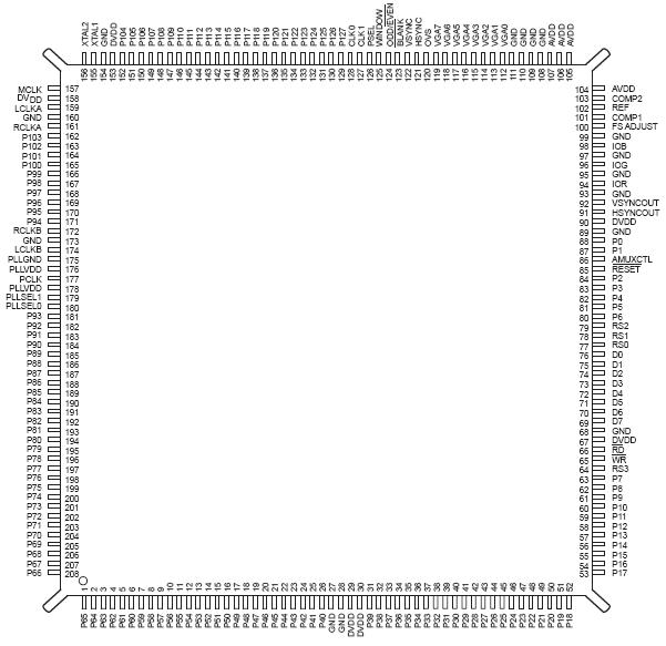
Pinout

  Connection Diagram


Specifications

Supply voltage, VDD (see Note 1) . . . . . . . . . . . . . . . . . . . . . . . . . . . . . . . . . . . . . . . . . . . . 7 V
Input voltage range, VI . . . . . . . . . . . . . . . . . . . . . . . . . . . . . . . . . . .0.5 V to VDD + 0.5 V
Analog output short-circuit duration to any power supply or common . . . . . . . . . unlimited
Operating free-air temperature range, TA . . . . . . . . . . . . . . . . . . . . . . . . . . . . 0°C to 70°C
Storage temperature range, Tstg . . . . . . . . . . . . . . . . . . . . . . . . . . . . . . . .65°C to 150°C
Junction temperature, TJ . . . . . . . . . . . . . . . . . . . . . . . . . . . . . . . . . . . . . . . . . . . . . .175°C
Case temperature for 10 seconds: PPA package . . . . . . . . . . . . . . . . . . . . . . . . . . . 260°C
Lead temperature 1,6 mm (1/16 inch) from case for 10 seconds . . . . . . . . . . . . . . . 260°C
† Stresses beyond those listed under "absolute maximum ratings" may cause permanent damage to the device. These
are stress ratings only, and functional operation of the device at these or any other conditions beyond those indicated
under "recommended operating conditions" is not implied. Exposure to absolute-maximum-rated conditions for
extended periods may affect device reliability.
NOTE 1: All voltage values are with respect to GND.


Description

A standard microprocessor interface is supported, giving the MPU direct access to the registers and memories of the TVP3033. The processor interface is controlled via read and write strobes (RD, WR), the four register select terminals RS(30) and the D(70) data terminals. A software selectable 8/6-function is used to select between an 8-bit or 6-bit wide data path to the color palette RAM and is provided in order to maintain VGA compatibility.

Table 21 shows the direct register map. These TVP3033 registers are addressed directly by the register select lines RS(30). Table 22 shows the indirect register map. The index for the indirect register map is loaded into the index register (direct register: 0000). This  TVP3033 register is also used as the palette RAM write address and cursor RAM write address. The indexed data register (direct register: 1010) is then used to read or write the register pointed to in the indirect register map. The index register does not post-increment following accesses to the indirect map.


Customers Who Bought This Item Also Bought

Margin,quality,low-cost products with low minimum orders. Secure your online payments with SeekIC Buyer Protection.
Optical Inspection Equipment
Cable Assemblies
Optoelectronics
Programmers, Development Systems
Industrial Controls, Meters
View more