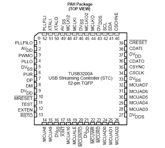
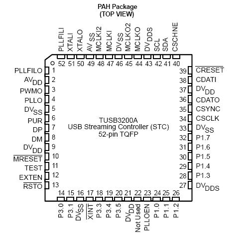
Features: • Universal Serial Bus (USB) • USB Specification version 1.1 compatible • USB Audio Class Specification 1.0 compatible • Integrated USB transceiver • Supports 12 Mb/s data rate (full speed) • Supports suspend/resume and remote wake-up • Supports ...
TUSB3200A: Features: • Universal Serial Bus (USB) • USB Specification version 1.1 compatible • USB Audio Class Specification 1.0 compatible • Integrated USB transceiver • Supports...
SeekIC Buyer Protection PLUS - newly updated for 2013!
268 Transactions
All payment methods are secure and covered by SeekIC Buyer Protection PLUS.
2.1 Architectural Overview
2.1.1 Oscillator and PLL
Using an external 6-MHz crystal, the TUSB3200A derives the fundamental 48-MHz internal clock signal using an on-chip oscillator and PLL. Using the PLL output, the other required clock signals are generated by the clock generator and adaptive clock generator.
2.1.2 Clock Generator and Sequencer Logic
Utilizing the 48-MHz input from the PLL, the clock generator logic generates all internal clock signals, except for the codec port interface master clock (MCLK) and serial clock (CSCLK) signals. The TUSB3200A internal clocks include the 48-MHz clock, a 24-MHz clock, a 12-MHz clock and a USB clock. The USB clock also has a frequency of 12-MHz.The USB clock is the same as the 12-MHz clock when the TUSB3200A is transmitting data and is derived from the data when the TUSB3200A is receiving data. To derive the USB clock when receiving USB data, the TUSB3200A utilizes an internal digital PLL (DPLL) that uses the 48-MHz clock.The sequencer logic controls the access to the SRAM used for the USB endpoint configuration blocks and the USB endpoint buffer space. The SRAM can be accessed by the MCU, USB buffer manager (UBM) or DMA channels. The sequencer controls the access to the memory using a round robin fixed priority arbitration scheme. This basically means that the sequencer logic generates grant signals for the MCU, UBM and DMA channels at a predetermined fixed frequency.
2.2 Device Operation
The operation of the TUSB3200A is explained in the following sections. For additional information on USB, refer to the universal serial bus Specification version 1.1.
2.2.1 Clock Generation
The TUSB3200A requires an external 6-MHz crystal and PLL loop filter components connected as shown in Figure 4-1 to derive all the clocks needed for both USB and codec operation. Using the low frequency 6-MHz crystal and generating the required higher frequency clocks internal to the IC is a major advantage regarding EMI.
2.2.2 Device Initialization
After a power-on reset is applied to the TUSB3200A device, the 8052 MCU will execute a boot loader program from the 4K byte boot ROM mapped to the program memory space. During device initialization, the boot loader program downloads the application program code from an external EEPROM through the I2C interface. This requires that a binary image of the application code be written to the 8K byte code RAM in the TUSB3200A device.All memory mapped registers are initialized to a default value as defined in Appendix A, MCU Memory and Memory-Mapped Registers. The TUSB3200A device powers up with a default function address of zero and disconnected from the USB.