TS5A4597

Features: ` Low ON-State Resistance (8 )` ON-State Resistance Flatness (1.5 )` Control Inputs Are 5.5-V Tolerant` Low Charge Injection (5 pC Max)` 450-MHz −3-dB Bandwidth at 25` Low Total Harmonic Distortion (THD) (0.04%)` 2-V to 5.5-V Single-Supply Operation` Specified at 5-V and 3.3-V Node...

product image

TS5A4597 Picture
SeekIC No. : 004528839 Detail

TS5A4597: Features: ` Low ON-State Resistance (8 )` ON-State Resistance Flatness (1.5 )` Control Inputs Are 5.5-V Tolerant` Low Charge Injection (5 pC Max)` 450-MHz −3-dB Bandwidth at 25` Low Total Harm...

floor Price/Ceiling Price

Part Number:
TS5A4597
Supply Ability:
5000

Price Break

  • Qty
  • 1~5000
  • Unit Price
  • Negotiable
  • Processing time
  • 15 Days
Total Cost: $ 0.00

SeekIC Buyer Protection PLUS - newly updated for 2013!

  • Escrow Protection.
  • Guaranteed refunds.
  • Secure payments.
  • Learn more >>

Month Sales

268 Transactions

Rating

evaluate  (4.8 stars)

Upload time: 2025/1/11

Payment Methods

All payment methods are secure and covered by SeekIC Buyer Protection PLUS.

Notice: When you place an order, your payment is made to SeekIC and not to your seller. SeekIC only pays the seller after confirming you have received your order. We will also never share your payment details with your seller.
Product Details

Description


Features:

` Low ON-State Resistance (8 )
` ON-State Resistance Flatness (1.5 )
` Control Inputs Are 5.5-V Tolerant
` Low Charge Injection (5 pC Max)
` 450-MHz −3-dB Bandwidth at 25
` Low Total Harmonic Distortion (THD) (0.04%)
` 2-V to 5.5-V Single-Supply Operation
` Specified at 5-V and 3.3-V Nodes
` −85-dB OFF Isolation at 1 MHz
` Latch-Up Performance Exceeds 100 mA Per JESD 78, Class II
` 0.5-nA Max OFF Leakage
` ESD Performance Tested Per JESD 22
    − 2000-V Human-Body Model (A114-B, Class II)
    − 1000-V Charged-Device Model (C101)
` TTL/CMOS-Logic Compatible


Application

· Sample-and-Hold Circuits
· Battery-Powered Equipment (Cellular Phones, PDAs)
· Audio and Video Signal Routing
· Communication Circuits
· PCMCIA Cards


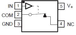
Pinout

  Connection Diagram


Specifications

MIN
MAX
UNIT
V+
Supply voltage range(3)
-0.3
6
V
VNO
VCOM
Analog voltage range(3) (4)
-0.3
V+ + 0.3
V
IK
Analog port diode current VNO, VCOM < 0
-50
mA
INO
ICOM
On-state switch current VNO, VCOM = 0 to V+
-20
20
mA
VI
Digital input voltage range(3) (4)
-0.3
6
V
IIK
Digital input clamp current VI < 0
-50
 
mA
I+
Continuous current through V+  
100
mA
IGND
Continuous current through GND -100
mA
JA
Package thermal impedance(5) DBV package  
206
/W
DCK package
252
Tstg
Storage temperature range
-65
150
(1) Stresses above these ratings may cause permanent damage. Exposure to absolute maximum conditions for extended
      periods may degrade device reliability. These are stress ratings only, and functional operation of the device at these or
      any other conditions beyond those specified is not implied.
(2) The algebraic convention, whereby the most negative value is a minimum and the most positive value is a maximum
(3) All voltages are with respect to ground, unless otherwise specified.
(4) The input and output voltage ratings may be exceeded if the input and output clamp-current ratings are observed.
(5) The package thermal impedance is calculated in accordance with JESD 51-7.


Description

The TS5A4597 is a single-pole single-throw (SPST) analog switch that is designed to operate from 2 V to 5.5 V. This device can handle both digital and analog
signals, and signals up to V+ can be transmitted in either direction.


Customers Who Bought This Item Also Bought

Margin,quality,low-cost products with low minimum orders. Secure your online payments with SeekIC Buyer Protection.
Hardware, Fasteners, Accessories
RF and RFID
Cables, Wires
Boxes, Enclosures, Racks
Fans, Thermal Management
Computers, Office - Components, Accessories
View more