Features: ` 1-A Low-Dropout Regulator With Enable
` Available in Fixed and Adjustable (1.2-V to 5.5-V) Versions
` High PSRR (53 dB at 10 kHz)
` Ultralow-Noise (40 VRMS, TPS79630)
` Fast Start-Up Time (50 s)
` Stable With a 1-F Ceramic Capacitor
` Excellent Load/Line Transient Response
` Very Low Dropout Voltage (250 mV at Full Load, TPS79630)
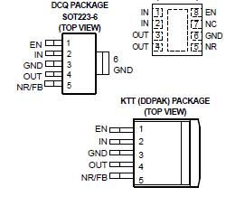
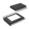
` 3 x 3 SON, 6-Pin SOT223-6, and 5-Pin DDPAK Packages
Application· RF: VCOs, Receivers, ADCs
· Audio
· Bluetooth™, Wireless LAN
· Cellular and Cordless Telephones
· Handheld Organizers, PDAsPinout Specifications
| |
UNIT
|
| VIN range |
-0.3 V to 6 V |
| VEN range |
-0.3 V to VIN + 0.3 V |
| VOUT range |
6 V |
| Peak output current |
Internally limited |
| ESD rating, HBM |
2 kV |
| ESD rating, CDM |
500 V |
| Continuous total power dissipation |
See Dissipation Ratings Table |
| Junction temperature range, TJ |
-40°C to 150°C |
| Storage temperature range, Tstg |
-65°C to 150°C |
(1) Stresses beyond those listed under absolute maximum ratings may cause permanent damage to the device. These are stress ratings only, and functional operation of the device at these or any other conditions beyond those indicated under recommended operating conditions is not implied. Exposure to absolute-maximum-rated conditions for extended periods may affect device reliability.
DescriptionThe TPS796xx family of low-dropout (LDO) low-power linear voltage regulators features high power supply rejection ratio (PSRR), ultralow-noise, fast start-up, and excellent line and load transient responses in small outline, 3 x 3 SON, SOT223-6, and 5-pin DDPAK packages. Each device TPS796xx in the family is stable with a small 1-F ceramic capacitor on the output. The family uses an advanced, proprietary BiCMOS fabrication process to yield extremely low dropout voltages (e.g., 250 mV at 1 A). Each device TPS796xx achieves fast start-up times (approximately 50 s with a 0.001-F bypass capacitor) while consuming very low quiescent.
(2u6rr5entA typical). Moreover, when the TPS796xx is placed in standby mode, the supply current is reduced to less than 1 A. The TPS79630 exhibits approximately 40 VRMS of output voltage noise at 3.0-V output, with a 0.1-F bypass capacitor. Applications with analog components that are noise sensitive, such as portable RF electronics, benefit from the high PSRR, low noise features, and the fast response time.

 TPS796xx Data Sheet


