Features: ·2-A Low-Dropout Voltage Regulator
·Available in 1.5-V, 1.8-V, 2.5-V, 3.3-V Fixed Output and Adjustable Versions
·Open Drain Power-On Reset With 100-ms Delay (TPS752xxQ)
·Open Drain Power-Good (PG) Status
·Output (TPS754xxQ)
·Dropout Voltage Typically 210 mV at 2 A (TPS75233Q)
·Ultralow 75-µA Typical Quiescent Current
·Fast Transient Response
·2% Tolerance Over Specified Conditions
·for Fixed-Output Versions
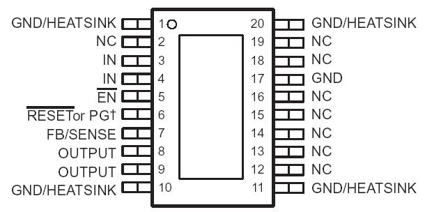
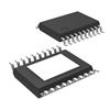
·20-Pin TSSOP (PWP) PowerPAD Package
·Thermal Shutdown ProtectionPinout Specifications
Input voltage range‡, VI . . . . . . . . . . . . . . . . . . . . . . . . . ..0.3 V to 6.0 V
Voltage range at EN . . . . . . . . . . . . . . . . . . . . . . . . . . . . ..0.3 V to 16.5 V
Maximum RESET voltage (TPS752xxQ) . . . . . . . . . . . . . . . . . . . . . . . .16.5 V
Maximum PG voltage (TPS754xxQ) . . . . . . . . . . . . . . . . . . . . . . . . . . .16.5 V
Peak output current . . . . . . . . . . . . . . . . . . . . . . . . . . . . . .Internally limited
Output voltage, VO (OUTPUT, FB) . . . . . . . . . . . . . . . . . . . . . . . . . . . . .5.5 V
Continuous total power dissipation . . . . . . . ..See dissipation rating tables
Operating virtual junction temperature range, TJ . . . . . .40°C to 125°C
Storage temperature range, Tstg . . . . . . . . . . . . . . . . . .65°C to 150°C
ESD rating, HBM . . . . . . . . . . . . . . . . . . . . . . . . . . . . . . . . . . . . . . . . . . 2 kV
† Stresses beyond those listed under "absolute maximum ratings" may cause permanent damage to the device. These are stress ratings only, and functional operation of the device at these or any other conditions beyond those indicated under "recommended operating conditions" is not implied. Exposure to absolute-maximum-rated conditions for extended periods may affect device reliability.
‡ All voltage values are with respect to network terminal ground.
DescriptionThe TPS75401Q are low dropout regulators with integrated power-on reset and power good (PG) functions respectively. These devices are capable of supplying 2 A of output current with a dropout of 210 mV (TPS75233Q, TPS75433Q). Quiescent current is 75 µA at full load and drops down to 1 µA when the device is disabled. TPS75401Q are designed to have fast transient response for larger load current changes.
Because the PMOS device TPS75401Q behaves as a low-value resistor, the dropout voltage is very low (typically 210 mV at an output current of 2 A for the TPS75x33Q) and is directly proportional to the output current. Additionally, since the PMOS pass element is a voltage-driven device, the quiescent current is very low and independent of output loading (typically 75 µA over the full range of output current, 1 mA to 2 A). These two key specifications of TPS75401Q yield a significant improvement in operating life for battery-powered systems.
The TPS75401Q is enabled when the EN pin is connected to a low-level input voltage. This LDO family also features a sleep mode; applying a TTL high signal to EN (enable) shuts down the regulator, reducing the quiescent current to 1 µA at TJ = 25°C.
The RESET (SVS, POR, or power on reset) output of the TPS752xxQ initiates a reset in microcomputer and microprocessor systems in the event of an undervoltage condition. An internal comparator in the TPS752xxQ monitors the output voltage of the regulator to detect an undervoltage condition on the regulated output voltage. When the output reaches 95% of its regulated voltage, RESET goes to a high-impedance state after a 100-ms delay. RESET goes to a logic-low state when the regulated output voltage is pulled below 95% (i.e., over load condition) of its regulated voltage.
The TPS75401Q has a power good terminal (PG) as an active high, open drain output, which can be used to implement a power-on reset or a low-battery indicator.
The TPS752xxQ or the TPS754xxQ are offered in 1.5-V, 1.8-V, 2.5-V, and 3.3-V fixed-voltage versions and in an adjustable version (programmable over the range of 1.5 V to 5 V). Output voltage tolerance is specified as a maximum of 2% over line, load, and temperature ranges. The TPS752xxQ and the TPS75401Q families are available in 20 pin TSSOP (PWP) packages.

 TPS75401Q Data Sheet


