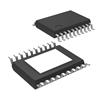
Features: · 1.8-V to 6-V Input Voltage Range · Integrated VCOM Buffer· High Voltage Switch to Isolate VGH· Gate Voltage Shaping of VGH· 2-A Internal MOSFET Switch· Main Output Vs up to 15 V With <1% Output Voltage Accuracy· Virtual Synchronous Converter Technology· Negative Regulated Charge Pum...
TPS65150PWP_1059472: Features: · 1.8-V to 6-V Input Voltage Range · Integrated VCOM Buffer· High Voltage Switch to Isolate VGH· Gate Voltage Shaping of VGH· 2-A Internal MOSFET Switch· Main Output Vs up to 15 V With <...
SeekIC Buyer Protection PLUS - newly updated for 2013!
268 Transactions
All payment methods are secure and covered by SeekIC Buyer Protection PLUS.
US $33.48 - 33.48 / Piece
Power Management IC Development Tools 2 batt cells
· 1.8-V to 6-V Input Voltage Range
· Integrated VCOM Buffer
· High Voltage Switch to Isolate VGH
· Gate Voltage Shaping of VGH
· 2-A Internal MOSFET Switch
· Main Output Vs up to 15 V With <1% Output Voltage Accuracy
· Virtual Synchronous Converter Technology
· Negative Regulated Charge Pump Driver VGL
· Positive Regulated Charge Pump Driver VGH
· Adjustable Power On Sequencing
· Adjustable Fault Detection Timing
· Gate Drive Signal for external isolation MOSFET
· Thermal Shutdown
· Available in TSSOP-24 Package
· Available in QFN-24 Package
· TFT LCD Displays for Notebooks
· TFT LCD Display for Monitor
· Car Navigation Display
over operating free-air temperature range (unless otherwise noted)(1)
UNIT | |
Voltages on pin VIN(2) |
0.3 V to 7 V |
Voltages on pin SUP |
0.3 V to 15.5 V |
Voltage on pin SW |
20 V |
Voltage on CTRL |
0.3 V to 7 V |
Voltage on GD |
15.5 V |
Voltage on CPI |
32V |
Continuous power dissipation |
See Dissipation Rating Table |
Operating junction temperature range |
40 to 150 |
Storage temperature range |
65 to 150 |
Lead temperature (soldering, 10 sec) |
260 |
(1) Stresses beyond those listed under absolute maximum ratings may cause permanent damage to the device. These are stress ratings only, and functional operation of the device at these or any other conditions beyond those indicated under recommended operating conditions is not implied. Exposure to absolute-maximum-rated conditions for extended periods may affect device reliability.
(2) All voltage values are with respect to network ground terminal.
The TPS65150PWP_1059472 offers a very compact and small power supply solution that provides all three voltages required by thin film transistor (TFT) LCD displays.
With an input voltage range of 1.8 V to 6.0 V the TPS65150PWP_1059472 is ideal for notebooks powered by a 2.5-V or 3.3-V input rail or monitor applications with a 5-V input voltage rail. Additionally the TPS65150 provides an integrated high current buffer to provide the VCOM voltage for the TFT backplane.
Two regulated adjustable charge pump driver of TPS65150PWP_1059472 provide the positive VGH and negative VGL bias voltages for the TFT. The device incorporates adjustable power on sequencing for VGL as well as for VGH. This avoids any additional external components to implement application specific sequencing. The TPS65150PWP_1059472 has an integrated high voltage switch to isolate VGH.