Features: ` Complete LTPS-LCD Bias Solution
` Triple Output Charge Pump Providing VCC at 16 mA, VDD at 2 mA, VSS at 1 mA
` 2.4 V to 5.5 V Input Voltage Range
` Fixed Output Voltages of 3.3 V, 7.5 V, −2.7 V or 5.0 V, 9.0 V, −3.0 V
` 50 A Typical Quiescent Current
` Less Than 1 A Shutdown Current
` Ultra-Low Ripple (VCC = 5 mV, Typical at 5 mA)
` Autonomous Boost for VCC Supply
` 1.5% Accuracy on Fixed VCC Output Voltage
` Sequential Power Control
` 24-Pin QFN Package (4 x 4)
Application· Small Form LTPS−LCD Displays
· PDAs, Pocket PCs
· Smart Phones
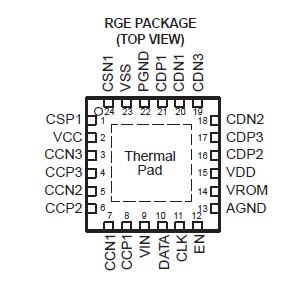
Pinout Specifications
| |
UNIT |
| Supply voltage VIN(2) |
-0.3 V to 7 V |
| Voltages on EN, MODE, FB, SW(2) |
−0.3 V to VIN + 0.3 V |
| Power dissipation (3) |
46/W |
| Virtual operation junction temperature, TJ |
−40° to 125 |
| Storage temperature range |
-65 to 150 |
| Lead temperature 1,6 mm (1/16 inch) from case for 10 seconds |
260 |
(1) Stresses beyond those listed under "absolute maximum ratings" may cause permanent damage to the device. These are stress ratings only, and functional operation of the device at these or any other conditions beyond those indicated under "recommended operating conditions" is not implied. Exposure to absolute-maximum-rated conditions for extended periods may affect device reliability.
(2) All voltage values are with respect to network ground terminal.
(3) The package thermal impedance is calculated in accordance with JESD 51−5.
DescriptionThe TPS65110/11 is a very compact power supply solution providing the three voltages required by many LTPS LCD displays.
All three regulated outputs of TPS65110/11 are generated using a charge pump topology.
The VCC charge pump provides precise, high efficiency, and very low ripple dc/dc conversion for the LCD analog power. The VCC boost ratio (x1.0, x1.33, x1.5, and x2.0) is automatically set based on input and output voltage conditions. The VCC output assures 16 mA of current by using three 0.22-F flying capacitors. If the required output current is smaller, smaller capacitors can be applied.
The VDD charge pump TPS65110/11 provides a higher positive voltage, and the VSS charge pump provides the negative output voltage. Power up/down sequences are internally set and are secured even in cases of sudden and abnormal VIN drop.
One of the most significant features of the TPS65110/11 is the ultra-low output voltage ripple, as the VCC charge pump achieves 5-mV output ripple voltage.

 TPS65110RGE_1060190 Data Sheet


