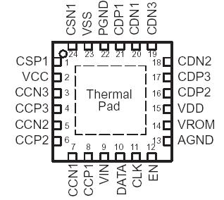
Features: Complete LTPS-LCD Bias SolutionTriple Output Charge Pump Providing VCC at 16 mA, VDD at 2 mA, VSS at 1 mA2.4 V to 5.5 V Input Voltage RangeFixed Output Voltages of 3.3 V, 7.5 V, −2.7 V or 5.0 V, 9.0 V, −3.0 V50 µA Typical Quiescent CurrentLess Than 1 µA Shutdown C...
TPS65110: Features: Complete LTPS-LCD Bias SolutionTriple Output Charge Pump Providing VCC at 16 mA, VDD at 2 mA, VSS at 1 mA2.4 V to 5.5 V Input Voltage RangeFixed Output Voltages of 3.3 V, 7.5 V, −2.7...
SeekIC Buyer Protection PLUS - newly updated for 2013!
268 Transactions
All payment methods are secure and covered by SeekIC Buyer Protection PLUS.
US $33.48 - 33.48 / Piece
Power Management IC Development Tools 2 batt cells
UNIT | |
Supply voltage at VIN (2) | −0.3 V to 7.0 V |
Input voltage at EN, CLK, DATA (2) | −0.3 V to VIN + 0.3 V |
Power dissipation (3) | 46°C/W |
Virtual operation junction temperature, TJ | −40°C to 125°C |
Storage temperature range | −65°C to 150°C |
Lead temperature 1,6 mm (1/16 inch) from case for 10 seconds | 260°C |
The TPS65110/11 is a very compact power supply solution providing the three voltages required by many LTPS LCD displays.
All three regulated outputs of TPS65110/11 are generated using a charge pump topology.
The VCC charge pump TPS65110/11 provides precise, high efficiency, and very low ripple dc/dc conversion for the LCD analog power. The VCC boost ratio (x1.0, x1.33, x1.5, and x2.0) is automatically set based on input and output voltage conditions. The VCC output assures 16 mA of current by using three 0.22-µF flying capacitors. If the required output current is smaller, smaller capacitors can be applied.
The VDD charge pump TPS65110/11 provides a higher positive voltage, and the VSS charge pump provides the negative output voltage. Power up/down sequences are internally set and are secured even in cases of sudden and abnormal VIN drop.
One of the most significant features of the TPS65110/11 is the ultra-low output voltage ripple, as the VCC charge pump achieves 5-mV output ripple voltage.