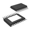
Features: · 2.7-V to 5.8-V Input Voltage Range· 1.6-MHz Fixed Switching Frequency· 3 Independent Adjustable Outputs· Main Output of up to 15 V With < 1% Output Voltage Accuracy · Negative Output Voltage Down to -12 V/20 mA · Positive Output Voltage up to 30 V/20 mA· Integrated VCOM Buffer· Auxi...
TPS65100: Features: · 2.7-V to 5.8-V Input Voltage Range· 1.6-MHz Fixed Switching Frequency· 3 Independent Adjustable Outputs· Main Output of up to 15 V With < 1% Output Voltage Accuracy · Negative Output ...
SeekIC Buyer Protection PLUS - newly updated for 2013!
268 Transactions
All payment methods are secure and covered by SeekIC Buyer Protection PLUS.
US $33.48 - 33.48 / Piece
Power Management IC Development Tools 2 batt cells
The TPS65100/05 offers a compact and small powersupply solution that provides all three voltages required by thin film transistor (TFT) LCD displays. The auxiliary linear regulator controller can be usedto generate a 3.3-V logic power rail for systemspowered by a 5-V supply rail only.
The main output, Vo1, is a 1.6-MHz, fixed-frequencyPWM boost converter providing the source drivevoltage for theLCD display. The device is available in two versions with different internal switch current limits to allow the use of asmaller external inductorwhen lower output power is required. The TPS65100has a typical switch current limit of 2.3 A, andthe TPS65105 has a typical switch current limit of 1.37 A.A fully integrated adjustable charge pumpdoubler/tripler provides the positive LCD gate drivevoltage. An externally adjustable negative charge pump provides the negative gate drive voltage. Dueto the high 1.6-MHz switching frequency of thecharge pumps, inexpensive and small 220-nF capacitors can be used.
The TPS65100/05 has an integrated VCOM buffer to power the LCD backplane. For LCD panels powered by 5 V only, the TPS65100/05 has a linear regulatorcontroller using an external transistor to provide aregulated 3.3-V output for the digital circuits. Formaximum safety, the entire device goes into shut- down as soon as one of the outputs is out of
regulation. The device can be enabled again bytoggling the input or the enable (EN) pin to GND.