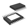
Features: ·High Efficiency, 550-mA, Adjustable-Output Buck Boost DC-DC Converter
· 6 High Performance LDO With Low Power Mode
·2 Analog Switches
·2 High Performance LDO
·3-Channel Selectable Output, 8-Bit Resolution D/A Converter
·12-Bit Resolution D/A Converter
· 3-Channel Clock Buffer of 26 MHz VCTCXO For Clock Reference
· 2 Serial Interface With 3-Wire
· Thermal Shut Down Protection
· Hot-Die Detection For Die Temperature Alert
· 5 mm × 5 mm, 0.5 mm Pitch MicroStar Juniortm PackageApplication· UMTS/WCDMA/GSM Cellular Phone
· Smart Phones
· Wireless ModemsSpecifications
| |
VALUE |
UNIT |
| Supply voltage |
VIO1V8 pin with respect to GND2 |
0.3 to 3.3 |
V |
| VBN1 pin with respect to GND1 |
0.3 to 5.5 |
V |
| VBN2 pin with respect to GND2 |
0.3 to 5.5 |
V |
| VBN3 pin with respect to GND3 |
0.3 to 5.5 |
V |
| VBN4 pin with respect to GND4 |
0.3 to 5.5 |
V |
| VBN5 pin with respect to GND5 |
0.3 to 5.5 |
V |
| VBDDP(2) pin with respect to DDGNDP(2) |
0.3 to 5.5 |
V |
| DDINA pin with respect to DDGNDA |
0.3 to 5.5 |
V |
| Input voltage range on REG_EN pin with respect to GND2 |
0.3 to 5.5 |
V |
| Input voltage range on PABIAS1, PA_FB and ERR pins with respect to DDGNDA |
0.3 to 5.5 |
V |
| Input voltage range(2) on L1 and L2 pins with respect to DDGNDP |
0.3 to 5.5 |
V |
| Input voltage range on other pins(3) |
0.3 to 5.5 |
V |
| Input voltage range on SYSCLK_IN pin with respect to GND6 |
0.3 to 3.3 |
V |
| Input voltage range on other input pins(4) |
0.3 to 3.3 |
V |
| Input voltage range on other pins(5) |
0.3 to 3.3 |
V |
| Peak LDO and SW output current(6) |
Internally Limited |
|
| Peak current of power path(2) on VBDDP, L1, L2 pins with respect to DDGNDP |
5 |
A |
| Storage temperature |
40 to 150 |
°C |
| Maximum junction temperature |
125 |
°C |
(1) Stresses beyond those listed under absolute maximum ratings may cause permanent damage to the device. These are stress ratings only and functional operation of the device at these or any other conditions beyond those indicated under recommended operating conditions is not implied. Exposure to absolute-maximum-rated conditions for extended periods may affect device reliability
(2) VBDDP is A4 and B4 pins, L1 is A5 and B5 pins, L2 is A7 and B7 pins, and DDGNDP is A6 and B6 pins.
(3) Pin is VTCXO with respect to GND3. Pins are VGGE1_V28, VGGE2_V28, and VGGE3_V28 with respect to GND5. Pin is VOUT with respect to DDGNDP. Pin is TEST with respect to DDGNDA.
(4) Pins are CCLK, CDATA, CSTB, TSPCLK, TSPDIN, TSPEN, CRESET, WRFON, TXON, TXONFST, TBNDSEL1, TBNDSEL2,
SYSCLK_EN and SYSCLK_EN2 with respect to GND2.
(5) Pins are AFC, PAVREF1, PAVREF2, and PAVREF3 with respect to GND1. Pins are SIN_SYSCLK1, SIN_SYSCLK2 and
SIN_SYSCLK3 with respect to GND6.
(6) LDO and SW OUTPUT are V11_V28TX, PA_VDD, V12_V28RX, V_LNA_FEM, V15_V18A , V13_V28A, VTCXO, VGGE1_V28, VGGE2_V28 and VGGE3_V28.
DescriptionThe TPS65040 is an advanced RF power management chip for cellular phones, providing a highly optimized solution for UMTS/WCDMA/GSM power amplifier applications. This solution improves efficiency by voltage control of the power amplifiers, saving power to prolong battery life. The TPS65040 features buck boost DC/DC converters suited for applications requiring up to 550-mA output current while dynamically adjusting output voltage from 0.8 V to 4.2 V with a fast settling time, high performance 8-channel LDO regulators, 8bit DAC, 12bit ADC and clock distribution buffers of 26 MHz VCTCXO. Each block can be controlled by serial interface and external pins. The TPS65040 offers material cost savings and small size, using a compact 5 mm×5 mm MicroStar Juniortm package.

 TPS65040 Data Sheet


