TPS65030

Features: ` 4 Regulated Output Voltages with 3% Tolerance Fractional Charge Pump for 5 V/100 mA Fractional Charge Pump for 1.5 V/200 mA Doubling Charge Pump With LDO Mode for 3.3 V/22 mA LDO for 1.8 V/60 mA` Switching Frequency 1 MHz` 3 V to 5 V Operating Input Voltage Range at VCC Pin` Sleep ...

product image

TPS65030 Picture
SeekIC No. : 004527198 Detail

TPS65030: Features: ` 4 Regulated Output Voltages with 3% Tolerance Fractional Charge Pump for 5 V/100 mA Fractional Charge Pump for 1.5 V/200 mA Doubling Charge Pump With LDO Mode for 3.3 V/22 mA LDO for...

floor Price/Ceiling Price

Part Number:
TPS65030
Supply Ability:
5000

Price Break

  • Qty
  • 1~5000
  • Unit Price
  • Negotiable
  • Processing time
  • 15 Days
Total Cost: $ 0.00

SeekIC Buyer Protection PLUS - newly updated for 2013!

  • Escrow Protection.
  • Guaranteed refunds.
  • Secure payments.
  • Learn more >>

Month Sales

268 Transactions

Rating

evaluate  (4.8 stars)

Upload time: 2025/1/11

Payment Methods

All payment methods are secure and covered by SeekIC Buyer Protection PLUS.

Notice: When you place an order, your payment is made to SeekIC and not to your seller. SeekIC only pays the seller after confirming you have received your order. We will also never share your payment details with your seller.
Product Details

Description


Features:

` 4 Regulated Output Voltages with 3% Tolerance
    Fractional Charge Pump for 5 V/100 mA
    Fractional Charge Pump for 1.5 V/200 mA
    Doubling Charge Pump With LDO Mode for 3.3 V/22 mA
    LDO for 1.8 V/60 mA
` Switching Frequency 1 MHz
` 3 V to 5 V Operating Input Voltage Range at VCC Pin
` Sleep Mode Sets Vout2 and Vout3 Into LDO Mode
` Sleep Mode Reduces Quiescent Current of Vout2, Vout3, and Vout4 to 8 mA Each
` internal Bus Switch
` Vbus Comparator
` Internal Soft Start Limits Inrush Current
` Low Input Current Ripple and Low EMI
` Overcurrent and Overtemperature Protected
` Undervoltage Lockout With Hysteresis
` Ultra-Small 2,5 mm x 2,7 mm Chip Scale Package Applications


Application

` Power Supply for USB OTG for:
   Cellular Phones
   Smart Phones
   PDAs
   Handheld PCs
   Digital Cameras
   Camcorders


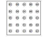
Pinout

  Connection Diagram


Specifications

  VALUE UNIT
VS Supply voltage at VIN, Vbus 0.3 to 7 V
Voltage at EN1, EN2, EN3, SLEEP, SW_EN1, SW_EN2, PG, Test SRP 0.3 V to VIN  
IO Output current at Vbus 200 mA
Output current at Vout2 40 mA
Output current at Vout3 300 mA
Output current at Vout4 100 mA
TJ Maximum junction temperature, 150 °C
TA Operating free-air temperature, 40 to 85 °C
Tstg Storage temperature, -65 to 150 °C


Description

The TPS65030 contains three charge pumps and one LDO to generate all supply voltages necessary for an USB On-The-Go (OTG) implementation using TUSB6010. The charge pumps are optimized for a single Li-Ion cell input or for 5 V from the USB bus.The input voltage range of TPS65030 is 3 V to 5 V for the battery voltage. High efficiency is achieved by using fractional conversion techniques for the charge pmuomdep.s Tinhecomcubrirneanttioncownittrhollead pocwhaerrgesavpinugmpssleeinp addition ensure low input current ripple and low EMI.Small size external ceramic capacitors are required to build a complete power supply solution. To reduce board space to a minimum, the TPS65030 switches at 1-MHz operating frequency, and is available in a small 25-ball lead free chip scale package (YZK).


Customers Who Bought This Item Also Bought

Margin,quality,low-cost products with low minimum orders. Secure your online payments with SeekIC Buyer Protection.
Cables, Wires
Power Supplies - Board Mount
Optical Inspection Equipment
Audio Products
Potentiometers, Variable Resistors
Soldering, Desoldering, Rework Products
View more