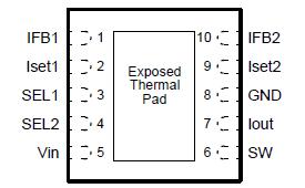
Features: · 3 V to 6 V Input Voltage Range· Two Outputs Each up to 27 V· 0.7 A Integrated Switch· Built-in Power Diode· 1.2 MHz Fixed PWM Frequency· Individually Programmable Output Current· Input-to-Output Isolation· Built-in Soft Start· Overvoltage Protection· Up to 83% Efficiency· Up to 30 kHz ...
TPS61150: Features: · 3 V to 6 V Input Voltage Range· Two Outputs Each up to 27 V· 0.7 A Integrated Switch· Built-in Power Diode· 1.2 MHz Fixed PWM Frequency· Individually Programmable Output Current· Input-t...
SeekIC Buyer Protection PLUS - newly updated for 2013!
268 Transactions
All payment methods are secure and covered by SeekIC Buyer Protection PLUS.
US $33.48 - 33.48 / Piece
Power Management IC Development Tools 2 batt cells
· 3 V to 6 V Input Voltage Range
· Two Outputs Each up to 27 V
· 0.7 A Integrated Switch
· Built-in Power Diode
· 1.2 MHz Fixed PWM Frequency
· Individually Programmable Output Current
· Input-to-Output Isolation
· Built-in Soft Start
· Overvoltage Protection
· Up to 83% Efficiency
· Up to 30 kHz PWM Dimming Frequency
· Availiable in a 10 Pin, 3 × 3 mm QFN Package
VALUE |
UNIT | |
Supply voltages on pin VIN(2) |
0.3 to 7 |
V |
Voltages on pins SEL1/2, ISET1/2(2) |
0.3 to 7 |
V |
Voltage on pin IOUT, SW, IFB1 and IFB2(2) |
30 |
V |
Continuous power dissipation |
See Dissipation Rating Table |
|
Operating junction temperature range |
40 to 150 |
°C |
Storage temperature range |
465 to 150 |
°C |
Lead temperature (soldering, 10 sec) |
260 |
°C |
(1) Stresses beyond those listed under absolute maximum ratings may cause permanent damage to the device. These are stress ratings only, and functional operation of the device at these or any other conditions beyond those indicated under recommended operating conditions is not implied. Exposure to absolute-maximum-rated conditions for extended periods may affect device reliability.
(2) All voltage values are with respect to network ground terminal.
The TPS61150/1 is a high frequency boost converter with two regulated current outputs for driving WLEDs. Each current output can be individually programmed through external resistors. There is dedicated selection pin for each output, so the two outputs can be turned on separately or simultaneously. The output current of TPS61150 can be reduced by a pulse width modulation (PWM) signal on the select pins or an analog voltage on the ISET pin, resulting in PWM dimming of the WLEDs. The boost regulator TPS61150 runs at 1.2 MHz fixed switching frequency to reduce output ripple and avoid audible noises associated with PFM control.
The two current outputs of TPS61150 are ideal for driving WLED backlight for the sub and main displays in clam shell phones. The two outputs can also be used for driving display and keypad backlights. When used together,the two outputs can drive up to 14 WLED for one large display.
In addition to the small inductor, small capacitor and 3 mm x 3 mm QFN package, the built-in MOSFET and diode of TPS61150 eliminate the need for any external power devices. Overall, the IC provides an extremely compact solution with high efficiency and plenty of flexibility.