Supply Current
:
Packaging
: Tube
Maximum Operating Temperature
: + 85 C
Function
: Step Up
Package / Case
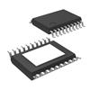
: HTSSOP-20 EP
Output Current
: 200 mA
Output Voltage
: 3 V
DescriptionThe TPS60125PWP is designed as one member of the TPS6012x family which are step-up, regulated charge pumps generate a 3.3-V or 3-V ±4% output voltage from a 1.8-V to 3.6-V input voltage (two alkaline, NiCd, or NiMH batteries). TPS60125PWP can deliver an output current of at least 200mA, all from a 2-V input. Four external capacitors are needed to build a complete high efficiency dc/dc charge pump converter. To achieve the high efficiency over a wide input voltage range, the charge pump automatically selects between a 1.5x or doubler conversion mode. From a 2-V input, all ICs can start with full load current. TPS60125PWP applications include applications powered by two battery cells, portable instruments, battery-powered microprocessor systems, miniature equipment, backup-battery boost converters, PDAs, organizers, laptops, MP-3 portable audio players, handheld instrumentation, medical instruments (e.g., glucose meters) and cordless phones.
TPS60125PWP has ten features. (1) High average efficiency over input voltage range because of special switching topology. (2) Minimum 200-mA output current from an input voltage range of 1.8V to 3.6V. (3) Regulated 3.3V or 3V ±4% output voltage. (4) No inductors required, low EMI. (5) Only four external components required. (6) 55-mA quiescent supply current. (7) 0.05mA shutdown current. (8) Load disconnected in shutdown. (9) Integrated low battery and power good detectors. (10) Evaluation module available. That are all the main features.
Some absolute maximum ratings of TPS60125PWP have been concluded into several points as follow. (1) Its input voltage range, VI (IN, OUT, ENABLE, FB, LBI, LBO/PG) would be from -0.3V to 5.5V. (2) Its differential input voltage, VID (C1+, C2+ to GND) would be from -0.3V to (VO + 0.3V). (3) Its differential input voltage, VID (C1, C2 to GND) would be from -0.3V to (VI + 0.3V). (4) Its cContinuous output current would be 300mA. (5) Its storage temperature range would be from -55°C to 150°C. (6) Its lead temperature 1,6 mm (1/16 inch) from case for 10s would be 260°C. (7) Its maximum junction temperature would be 150°C. And so on. If you have any question or suggestion or want to know more information about TPS60125PWP please contact us for details. Thank you!
Parameters: | Technical/Catalog Information | TPS60125PWP |
| Vendor | Texas Instruments |
| Category | Integrated Circuits (ICs) |
| Type | Switched Capacitor (Charge Pump), Step-Up (Boost) |
| Number of Outputs | 1 |
| Voltage - Input | 1.8 ~ 3.6 V |
| Voltage - Output | 3V |
| Current - Output | 200mA |
| Power - Output | 700mW |
| Package / Case | 20-TSSOP Exposed Pad, 20-eTSSOP, 20-HTSSOP |
| Packaging | Tube |
| Internal Switch(s) | Yes |
| Synchronous | No |
| Rds (On) | - |
| Operating Temperature | -40°C ~ 85°C |
| Frequency - Switching | 320kHz |
| Drawing Number | 296; 4073225; PWP; 14, 16, 20, 24, 28 |
| Lead Free Status | Lead Free |
| RoHS Status | RoHS Compliant |
| Other Names | TPS60125PWP
TPS60125PWP
296 10949 5 ND
296109495ND
296-10949-5
|

 TPS60125PWP Data Sheet


