TPS56302

Features: `2.8 V 5.5 V Input Voltage Range`Programmable Dual Output Controller Supports Popular DSP, FPGA and Microcontroller Core and I/O Voltages Switching Regulator Controls I/O Voltage Low Dropout Controller Regulates Core Voltage`Adjustable Slow-Start for Simultaneous Powerup of Both Outputs...

product image

TPS56302 Picture
SeekIC No. : 004526954 Detail

TPS56302: Features: `2.8 V 5.5 V Input Voltage Range`Programmable Dual Output Controller Supports Popular DSP, FPGA and Microcontroller Core and I/O Voltages Switching Regulator Controls I/O Voltage Low Drop...

floor Price/Ceiling Price

Part Number:
TPS56302
Supply Ability:
5000

Price Break

  • Qty
  • 1~5000
  • Unit Price
  • Negotiable
  • Processing time
  • 15 Days
Total Cost: $ 0.00

SeekIC Buyer Protection PLUS - newly updated for 2013!

  • Escrow Protection.
  • Guaranteed refunds.
  • Secure payments.
  • Learn more >>

Month Sales

268 Transactions

Rating

evaluate  (4.8 stars)

Upload time: 2025/1/11

Payment Methods

All payment methods are secure and covered by SeekIC Buyer Protection PLUS.

Notice: When you place an order, your payment is made to SeekIC and not to your seller. SeekIC only pays the seller after confirming you have received your order. We will also never share your payment details with your seller.
Product Details

Description


Features:

`2.8 V 5.5 V Input Voltage Range
`Programmable Dual Output Controller Supports Popular DSP, FPGA and Microcontroller Core and I/O Voltages
Switching Regulator Controls I/O Voltage
Low Dropout Controller Regulates Core Voltage
`Adjustable Slow-Start for Simultaneous Powerup of Both Outputs
`Power Good Output Monitors Both Outputs
`Fast Ripple Regulator Reduces Bulk Capacitance for Lower System Costs
`±1.5% Reference Voltage Tolerance
`Efficiencies Greater Than 90%
`Overvoltage, Undervoltage, and Adjustable Overcurrent Protection
`Drives Logic Level N-Channel MOSFETs Through Entire Input Voltage Range
`Evaluation Module TPS56302EVM163 Available


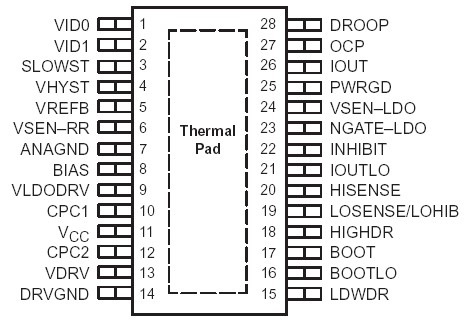
Pinout

  Connection Diagram


Specifications

Supply voltage range, VCC (see Note1)  . . . . . . . . . . . . . . . . . . . . . . . . . . . . . .. . .0.3 V to 6 V
Input voltage range: VDRV . . . . . . . . . . . . . . . . . . . . . . . . . . . . . . . . . . . . . . . .  . .0.3 V to 7 V
                                  BOOT to DRVGND (High-side Driver ON)  . . . . . . . . . . .  . . .0.3 V to 15 V 
                                  BOOT to BOOTLO  . . . . . . . . . . . . . . . . . . . . . . . . . . . . . . . . .0.3 V to 7 V
                                  BOOT to HIGHDRV . . . . . . . . . . . . . . . . . . . . . . . . . . . . . . . . .0.3 V to 7 V 
                                  BOOTLO to DRVGND  . . . . . . . . . . . . . . . . . . . . . . . . . . . . . .0.5 V to 15 V
                                  DRV to DRVGND . . . . . . . . . . . . . . . . . . . . . . . . . . . . . . . .  . .0.3 V to 7 V 
                                  BIAS to ANAGND. . . . . . . . . . . . . . . . . . . . . . . . . . . . . . . . . . 0.3 V to 7 V
                                  INHIBIT . . . . . . . . . . . . . . . . . . . . . . . . . . . . . . . . . . . . . . . . .0.3 V to 7 V 
                                  DROOP  . . . . . . . . . . . . . . . . . . . . . . . . . . . . . . . . . .0.3 V to VCC + 0.3 V
                                  OCP . . . . . . . . . . . . . . . . . . . . . . . . . . . . . . . . . . . . . . . . . .  .0.3 V to 7 V 
                                  VID0, VID1 (tri-level terminals)  . . . . . . . . . . . .. . .0.3 V to VBIAS + 0.3 V
                                  PWRGD  . . . . . . . . . . . . . . . . . . . . . . . . . . . . . . . . . . . . . . . . 0.3 V to 6 V 
                                  LOSENSE, LOHIB . . . . . . . . . . . . . . . . . . . . . . . . . . . . . . . . .0.5 V to 14 V 
                                  IOUTLO  . . . . . . . . . . . . . . . . . . . . . . . . . . . . . . . . . . . . . . . .0.3 V to 14 V
                                  HISENSE . . . . . . . . . . . . . . . . . . . . . . . . . . . . . . . . . . . .. . . . .0.3 V to 7 V 
                                  VSENLDO  . . . . . . . . . . . . . . . . . . . . . . . . . . . . . . .  . . . . . . 0.3 V to 6 V
                                  VSENRR . . . . . . . . . . . . . . . . . . . . . . . . . . . . . . . . . . . . . . . 0.3 V to 6 V
Voltage difference between ANAGND and DRVGND  . . . . . . . . . . . . . . . . . . . . . . . . . . . .±300 mV
Continuous total power dissipation  . . . . . . . . . . . . . . . . . . . . .  . . .See Dissipation Rating Table
Operating junction temperature range, TJ  . . . . . . . . . . . . . . .. . . . . . . . . . . . .40°C to 125°C
Storage temperature range, Tstg . . . . . . . . . . . . . . . . . . . . . . . . . . . . . . . .. . . 65°C to 150°C
Lead temperature soldering 1,6 mm (1/16 inch) from case for 10 seconds  . . . . .  . . . . . .300°C
NOTE 1: Unless otherwise specified, all voltages are with respect to ANAGND.


Description

The high-performance TPS56302 synchronous-buck regulator provides two supply voltages to power the core and I/O of digital signal processors. The TPS56302 is identical to the TPS56300 except that the reference voltages of the LDO and switching regulator have been reversed. The switching regulator, using hysteretic control with droop compensation, supports high current and efficiency for the I/O and other peripheral components. The LDO controller, suitable for powering the core voltage, drives an external N-channel power MOSFET and functions as an LDO regulator and as a power distribution switch.

To promote better system reliability during power up, voltage sequencing and protection are controlled such that the core and I/O power up together with the same slow-start voltage. At power down, the LDO and ripple regulator are discharged towards ground for added protection. The TPS56302 also includes inhibit, slow-start, and under-voltage lockout features to aide in controlling power sequencing. A tri-level voltage identification definition (VID) sets both regulated voltages to any of 9 preset voltage pairs from 1.3 V to 3.3 V. Other voltages are possible by implementing an external voltage divider. Strong MOSFET drivers, with a typical peak current rating of 2-A sink and source are included on chip, which allows paralleling MOSFETs to be driven and allowing higher current to be controlled. The high-side driver TPS56302 features a floating bootstrap driver with an internal bootstrap synchronous rectifier. Many protection features are incorporated within the TPS56302 to ensure better system integrity. An open-drain output power good status circuit monitors both output voltages, and is pulled low if either output falls below the threshold. An over current shutdown circuit protects the high-side power MOSFET against short-to-ground faults, while over voltage protection turns off the output drivers and LDO controller if either output exceeds its threshold. Under voltage protection turns off the high-side and low-side MOSFET drivers and the LDO controller if either output is 25% below VREF. Lossless current-sensing is implemented by detecting the drain-source voltage drop across the high-side power MOSFET while it is conducting. The TPS56302 is fully compliant with TI DSP power requirements.


Customers Who Bought This Item Also Bought

Margin,quality,low-cost products with low minimum orders. Secure your online payments with SeekIC Buyer Protection.
Hardware, Fasteners, Accessories
Prototyping Products
DE1
Power Supplies - External/Internal (Off-Board)
LED Products
Sensors, Transducers
View more