TPS5615

Features: ·±1% Reference Over Full Operating Temperature Range·Synchronous Rectifier Driver for >90% Efficiency·Fixed Output Voltage Options of 1.5 V,1.8 V, 2.5 V, and 3.3 V·User-Selectable Hysteretic-Type Control·Low Supply Current . . . 3 mA Typ·11.4-V to 13-V Input Voltage Range, VCC·Power G...

product image

TPS5615 Picture
SeekIC No. : 004526949 Detail

TPS5615: Features: ·±1% Reference Over Full Operating Temperature Range·Synchronous Rectifier Driver for >90% Efficiency·Fixed Output Voltage Options of 1.5 V,1.8 V, 2.5 V, and 3.3 V·User-Selectable Hyste...

floor Price/Ceiling Price

Part Number:
TPS5615
Supply Ability:
5000

Price Break

  • Qty
  • 1~5000
  • Unit Price
  • Negotiable
  • Processing time
  • 15 Days
Total Cost: $ 0.00

SeekIC Buyer Protection PLUS - newly updated for 2013!

  • Escrow Protection.
  • Guaranteed refunds.
  • Secure payments.
  • Learn more >>

Month Sales

268 Transactions

Rating

evaluate  (4.8 stars)

Upload time: 2025/1/11

Payment Methods

All payment methods are secure and covered by SeekIC Buyer Protection PLUS.

Notice: When you place an order, your payment is made to SeekIC and not to your seller. SeekIC only pays the seller after confirming you have received your order. We will also never share your payment details with your seller.
Product Details

Description


Features:

·±1% Reference Over Full Operating Temperature Range
·Synchronous Rectifier Driver for >90% Efficiency
·Fixed Output Voltage Options of 1.5 V,1.8 V, 2.5 V, and 3.3 V
·User-Selectable Hysteretic-Type Control
·Low Supply Current . . . 3 mA Typ
·11.4-V to 13-V Input Voltage Range, VCC
·Power Good Output
·Programmable Soft-Start
·Overvoltage/Overcurrent Protection
·Active Deadtime Control


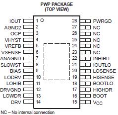
Pinout

  Connection Diagram


Specifications

Supply voltage range, VCC (see Note 1) . . . . . . . . . . . . . . . . . . . . . . . . . . . . . 0.3 to 14 V
Input voltage range: BOOT to DRVGND (high-side driver ON) . . . . . . . . . . . . . 0.3 to 30 V
                                 BOOT to HIGHDRV . . . . . . . . . . . . . . . . . . .  . . . . . . . . . . 0.3 to 15 V
                                 BOOT to BOOTLO . . . . . . . . . . . . . . . . . . . . . . . . . . . . . . 0.3 to 15 V
                                 INHIBIT, LODRV . . . . . . . . . . . . . . . . . . . . . . . . . . . . . . . 0.3 to 7.3 V
                                 PWRGD, OCP  . . . . . . . . . . . . . . . . . . . . . . . . . . . . . . . . . . 0.3 to 7 V
                                 LOHIB, LOSENSE, IOUTLO, HISENSE   . . . .  . . . . . . . . . . 0.3 to 14 V
                                 VSENSE . . . . . . . . . . . . . . . . . . . . . . . . .  . . . . . . . . . . . . . 0.3 to 5 V
Voltage difference between ANAGND and DRVGND . . . . . . . .. . . . . . . . . . . . . . . . . . ±0.5 V
Output current, VREFB . . . . . . . . . . . . . . . . . . . . . . . . . . .  . . . . . . . . . . . . . . . . . . . . 0.5 mA
Short circuit duration, DRV . . . . . . . . . . . . . . . . . . . . . . . . . . . . . . . . . . . . . . . . . Continuous
Continuous total power dissipation . . . . . . . . . . . . . . .  . . . . . See Dissipation Rating Table
Operating junction temperature range, TJ . . . . . . . . . .  . . . . . . . . . . . . . . . . . . 0 to 125
Storage temperature range, Tstg . . . . . . . . . . . . . . . . . . . . . . .. . . . . . . . . . . 65to 150
Lead temperature soldering 1,6 mm (1/16 inch) from case for 10 seconds . . . . . . . . . 260
† Stresses beyond those listed under "absolute maximum ratings" may cause permanent damage to the device. These are stress ratings only, and functional operation of the device at these or any other conditions beyond those indicated under "recommended operating conditions" is not implied. Exposure to absolute-maximum-rated conditions for extended periods may affect device reliability.
NOTE 1: Unless otherwise specified, all voltages are with respect to ANAGND.


Description

The TPS5615 family of synchronous-buck regulator controllers provides an ccurate supply voltage to DSPs. The output voltage is internally set by a resistive divider with an accuracy of 1% over the full operating temperature range. A hysteretic controller with user-selectable hysteresis is used to dramatically reduce overshoot and undershoot caused by load transients. Propagation delay from the omparator inputs to the output drivers is less than 250 ns. Overcurrent shutdown and crossover protection for the output drivers of TPS5615 combine to eliminate destructive faults in the output FETs. PWRGD monitors the output voltage and pulls the open-collector output low when the output drops below 93% of the nominal output voltage. An overvoltage circuit disables the output drivers if the output voltage rises 15% above the nominal value. The inhibit pin can be used to control power sequencing. Inhibit and undervoltage lockout assures that the 12-V supply oltage and system supply voltage (5 V or 3.3 V) are within proper operating limits before the controller starts. The output driver circuits of TPS5615 include 2-A drivers with internal 8-V gate-voltage regulators that can easily provide sufficient power for today's high-powered DSPs. The high-side driver can be configured either as a ground-referenced driver or as a floating bootstrap driver. The TPS5615 family is available in a 28-pin TSSOP PowerPadE package. It operates over a junction temperature range of 0 to 125


Customers Who Bought This Item Also Bought

Margin,quality,low-cost products with low minimum orders. Secure your online payments with SeekIC Buyer Protection.
Sensors, Transducers
Soldering, Desoldering, Rework Products
Memory Cards, Modules
Computers, Office - Components, Accessories
Cables, Wires - Management
View more