Features: ` Single-Channel, 5-V Controller
` Synchronous-Rectifier Drivers for Greater Than 90% Efficiency
` Useable for All Common DSP Supply Voltages Popular Output Voltage Options Set With Program Pins
` EVM Available
` Ideal for Applications With Current Ranges From 3 A to 30 A.
` Hysteretic Control Technique Enables Fast Transient Response - Ideal for 'C6000 or Multiple 'C5000 Applications
` Low Supply Current
3 mA in Operation
90 mA in Standby
` Power Good Output
` 28-Pin TSSOP PowerPADE Package
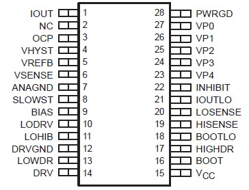
Pinout Specifications
absolute maximum ratings over operating virtual junction temperature (unless otherwise noted)†
Supply voltage range, VCC (see Note1), BIAS, DRV . . . . . . . . . . . . . . . . . . . 0.3 V to 7 V
Input voltage range: BOOT to DRVGND (High-side Driver ON) . . . . . . . . . . 0.3 V to 30 V
BOOT to HIGHDRV . . . . . . . . . . . . . . . . . . . . . . . . . . . . . . . . . . . . . . . . . . . . 0.3 V to 15 V
BOOT to BOOTLO . . . . . . . . . . . . . . . . . . . . . . . . . . . . . . . . . . . . . . . . . . . . .0.3 V to 15 V
INHIBIT, VPx, LODRV . . . . . . . . . . . . . . . . . . . . . . . . . . . . . . . . . . . . . . . . . .0.3 V to 7.3 V
PWRGD, OCP . . . . . . . . . . . . . . . . . . . . . . . . . . . . . . . . . . . . . . . . . . . . . . . . . 0.3 V to 7 V
LOHIB, LOSENSE, IOUTLO, HISENSE . . . . . . . . . . . . . . . . . . . . . . . . . . . . . . . 0.3 V to 7 V
VSENSE . . . . . . . . . . . . . . . . . . . . . . . . . . . . . . . . . . . . . . . . . . . . . . . . . . . . . 0.3 V to 5 V
Voltage difference between ANAGND and DRVGND . . . . . . . . . . . . . . . . . . . . . . . . . ±0.5 V
Output current, VREFB . . . . . . . . . . . . . . . . . . . . . . . . . . . . . . . . . . . . . . . . . . . . . . . 0.5 mA
Continuous total power dissipation . . . . . . . . . . . . . . . . . . . See Dissipation Rating Table
Operating virtual junction temperature range, TJ . . . . . . . . . . . . . . . . . . . . . . 0 to 125
Storage temperature range, Tstg . . . . . . . . . . . . . . . . . . . . . . . . . . . . . . . . 65 to 150
Lead temperature soldering 1,6 mm (1/16 inch) from case for 10 seconds . . . . . . . 260
† Stresses beyond those listed under "absolute maximum ratings" may cause permanent damage to the device. These are stress ratings only, and functional operation of the device at these or any other conditions beyond those indicated under "recommended operating conditions" is not implied. Exposure to absolute-maximum-rated conditions for extended periods may affect device reliability.
DescriptionThe TPS56100 is a high-efficiency synchronous-buck regulator controller which provides an accurate programmable supply voltage to low-voltage digital signal processors, such as the 'C6x and 'C54x DSPs. An internal 5-bit DAC is used to program the reference voltage from 1.3 V to 2.6 V. Higher output voltages can be implemented using an external input resistive divider. The TPS56100 uses a fast hysteretic control method that provides a quick transient response.
The propagation delay of TPS56100 from the comparator input to the output driver is less than 300 ns, even at maximum output current. Overcurrent shutdown and crossover protection combine to eliminate destructive faults in the output MOSFETs, thereby protecting the processor during operation. The slowstart current source is proportional to the reference voltage, thereby eliminating variation of the slowstart timing when changes are made to the output voltage. When the output drops to less than 93% of the nominal output voltage, PWRGD will pull the open-drain output low. The overvoltage circuit will disable the output drivers if the output voltage rises more than 15% above the nominal output voltage. The TPS56100 also includes an inhibit input to control power sequencing and undervoltage lockout thereby insuring the 5-V supply is within limits before the controller starts. The 2-A MOSFET drivers of TPS56100 can power multiple MOSFETs in parallel to drive single or multiple DSPs and load currents up to 30 A. The high-side driver can be configured as a ground-referenced driver or as a floating bootstrap driver with the included internal bootstrap Schottky diode.
The TPS56100 is available in a 28-pin TSSOP PowerPAD package, which increases thermal efficiency and eliminates bulky heat sinks.

 TPS56100 Data Sheet


