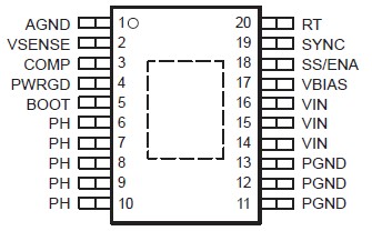
Features: · Integrated MOSFET Switches for High Efficiency at 1.5-A Continuous Output Source or Sink Current
· 0.9-V to 3.3-V Adjustable Output Voltage With 1% Accuracy
· Externally Compensated for Design Flexibility
· Fast Transient Response
· Wide PWM Frequency: Fixed 350 kHz, 550 kHz, or Adjustable 280 kHz to 700 kHz
· Load Protected by Peak Current Limit and Thermal Shutdown
· Integrated Solution Reduces Board Area and Total Cost
Application· Low-Voltage, High-Density Systems With Power Distributed at 5 V or 3.3 V
· Point of Load Regulation for High Performance DSPs, FPGAs, ASICs, and Microprocessors
· Broadband, Networking, and Optical Communications Infrastructure
· Portable Computing/Notebook PCs
Pinout Specifications
| |
TPS54010 |
UNIT |
| Input voltage range, VI |
VIN, SS/ENA, SYNC |
0.3 to 7 |
V |
| RT |
0.3 to 6 |
V |
| VSENSE |
0.3 to 4 |
V |
| BOOT |
0.3 to 17 |
V |
| Output voltage range, VO |
VBIAS, COMP, PWRGD |
0.3 to 7 |
V |
| PH |
0.6 to 10 |
V |
| Source current, IO |
PH |
Internally limited |
| COMP, VBIAS |
6 |
mA |
| Sink current |
PH |
|
A |
| COMP |
6 |
mA |
| SS/ENA, PWRGD |
10 |
mA |
| Voltage differential |
AGND to PGND |
±0.3 |
V |
| Continuous power dissipation |
See Power Dissipation
Rating Table |
| Operating virtual junction temperature range, TJ |
40 to 125 |
|
| Storage temperature, Tstg |
−65 to 150 |
|
| Lead temperature 1,6 mm (1/16 inch) from case for 10 seconds |
260 |
|
(1) Stresses beyond those listed under "absolute maximum ratings" may cause permanent damage to the device. These are stress ratings only, and functional operation of the device at these or any other conditions beyond those indicated under "recommended operating conditions" is not implied. Exposure to absolute-maximum-rated conditions for extended periods may affect device reliability.
DescriptionAs members of the SWIFT family of dc/dc regulators, the TPS54110 low-input-voltage high-output-current synchronous-buck PWM converter integrates all required active components. Included on the substrate with the listed features are a true, high-performance, voltage error amplifier that provides high performance under transient conditions; an undervoltage-lockout circuit to prevent start-up until the input voltage reaches 3 V; an internally and externally set slow-start circuit to limit in-rush currents; and a power-good output useful for processor/logic reset, fault signaling, and supply sequencing.
The TPS54110 device is available in a thermally enhanced 20-pin TSSOP (PWP) PowerPADTM package, which eliminates bulky heatsinks. TI provides evaluation modules and the SWIFT designer software tool to aid in quickly achieving high-performance power supply designs to meet aggressive equipment development cycles.

 TPS54110PWP_1059467 Data Sheet


