Features: ` 700 KHz Operation
` 1.25 MHz Operation With External Driver
` 1.5% Reference Over Full Operating Temperature Range
` Synchronous Rectifier Driver for Greater Than 90% Efficiency
` Programmable Reference Voltage Range of 1.3 V to 3.5 V
` UserSelectable Hysteretic Type Control
` Droop Compensation for Improved Load Transient Regulation
` Adjustable Overcurrent Protection
` Programmable Softstart
` Overvoltage Protection
` Active Deadtime Control
` Power Good Output
` Internal Bootstrap Schottky Diode
` Low Supply Current . . . 3-mA Typ
` Reduced System Component Count and Size
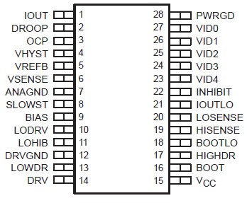
Pinout Specifications
absolute maximum ratings over operating virtual junction temperature (unless otherwise noted)†
Supply voltage range, VCC (see Note1) . . . . . . . . . . . . . . . . . . . . . . . . . . . 0.3 V to 14 V
Input voltage range: BOOT to DRVGND (High-side Driver ON) . . . . . . . . . . 0.3 V to 30 V
BOOT to HIGHDRV . . . . . . . . . . . . . . . . . . . . . . . . . . . . . . . . . . . . . . . . . . . . 0.3 V to 15 V
BOOT to BOOTLO . . . . . . . . . . . . . . . . . . . . . . . . . . . . . . . . . . . . . . . . . . . . . 0.3 V to 15 V
INHIBIT, VIDx, LODRV . . . . . . . . . . . . . . . . . . . . . . . . . . . . . . . . . . . . . . . . . 0.3 V to 7.3 V
PWRGD, OCP, DROOP . . . . . . . . . . . . . . . . . . . . . . . . . . . . . . . . . . . . . . . . . . 0.3 V to 7 V
LOHIB, LOSENSE, IOUTLO, HISENSE . . . . . . . . . . . . . . . . . . . . . . . . . . . . . . 0.3 V to 14 V
VSENSE . . . . . . . . . . . . . . . . . . . . . . . . . . . . . . . . . . . . . . . . . . . . . . . . . . . . . 0.3 V to 5 V
Voltage difference between ANAGND and DRVGND . . . . . . . . . . . . . . . . . . . . . . . . . ±0.5 V
Output current, VREFB . . . . . . . . . . . . . . . . . . . . . . . . . . . . . . . . . . . . . . . . . . . . . . . 0.5 mA
Short circuit duration, DRV . . . . . . . . . . . . . . . . . . . . . . . . . . . . . . . . . . . . . . . . Continuous
Continuous total power dissipation . . . . . . . . . . . . . . . . . . . . See Dissipation Rating Table
Operating virtual junction temperature range, TJ . . . . . . . . . . . . . . . . . . . . . . . 0 to 125
Storage temperature range, Tstg . . . . . . . . . . . . . . . . . . . . . . . . . . . . . . . . . 65 to 150
Lead temperature soldering 1,6 mm (1/16 inch) from case for 10 seconds . . . . . . . . . 260
† Stresses beyond those listed under "absolute maximum ratings" may cause permanent damage to the device. These are stress ratings only, and functional operation of the device at these or any other conditions beyond those indicated under "recommended operating conditions" is not implied. Exposure to absolute-maximum-rated conditions for extended periods may affect device reliability.
NOTE 1: Unless otherwise specified, all voltages are with respect to ANAGND.
DescriptionThe TPS5211 is a hysteretic regulator controller which provides an accurate, programmable supply voltage to microprocessors. An internal 5-bit DAC is used to program the reference voltage to within a range of 1.3 V to 3.5 V. The output voltage of TPS5211 can be set to equal the reference voltage or some multiple of the reference voltage.
A hysteretic controller with user-selectable hysteresis and programmable droop compensation of TPS5211 is used to dramatically reduce overshoot and undershoot caused by load transients. Propagation delay from the comparator inputs to the output drivers is less than 250 ns. Overcurrent shutdown and crossover protection for the output drivers combine to eliminate destructive faults in the output FETs. The softstart current source of TPS5211 is proportional to the reference voltage, thereby eliminating variation of the softstart timing when changes are made to the output voltage. PWRGD monitors the output voltage and pulls the open-collector output low when the output drops 7% below the nominal output voltage. An overvoltage circuit of TPS5211 disables the output drivers if the output voltage rises 15% above the nominal value. The inhibit pin can be used to control power sequencing.
Inhibit and undervoltage lockout of TPS5211 assures the 12-V supply voltage and system supply voltage (5 V or 3.3 V) is within proper operating limits before the controller starts. Single-supply (12 V) operation is easily accomplished using a low-current divider for the required 5-V signals. The output driver circuits of TPS5211 include 2-A drivers with internal 8-V gate-voltage regulators. The high-side driver can be configured either as a ground-referenced driver or as a floating bootstrap driver. The TPS5211 is available in a 28-pin TSSOP PowerPADE package. It operates over a junction temperature range of 0 to 125.

 TPS5211 Data Sheet


