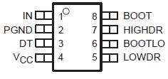
Features: `Floating Bootstrap or Ground-Reference High-Side Driver`Active Deadtime Control`50-ns Max Rise/Fall Times With 3.3-nF Load`2-A Min Peak Output Current`4.5-V to 15-V Supply Voltage Range`TTL-Compatible Inputs`Internal Schottky Bootstrap Diode`Low Supply Current . . . 3 mA Typ`Ideal for H...
TPS2836: Features: `Floating Bootstrap or Ground-Reference High-Side Driver`Active Deadtime Control`50-ns Max Rise/Fall Times With 3.3-nF Load`2-A Min Peak Output Current`4.5-V to 15-V Supply Voltage Range`T...
SeekIC Buyer Protection PLUS - newly updated for 2013!
268 Transactions
All payment methods are secure and covered by SeekIC Buyer Protection PLUS.
US $.42 - .86 / Piece
Power Switch ICs - USB Sgl Channel,Crnt-Ltd USB Pwr Dist Switch
US $.28 - .3 / Piece
Power Switch ICs - USB Sgl Channel,Crnt-Ltd USB Pwr Dist Switch
US $.53 - .86 / Piece
Power Switch ICs - USB SGL CH,CURRENT-LTD USB PWR DISTR SWITCH
Supply voltage range, VCC (see Note 1) . . . . . . . . . . . . . . . . . . . . . . . . . . . . . . . . . . . . . . . . . . . . . 0.3 V to 16 V
Input voltage range:BOOT to PGND (high-side driver ON) . . . . . . . . . . . . . . . . . . . . . . . . . . . . . 0.3 V to 30 V
BOOTLO to PGND . . . . . . . . . . . . . . . . . . . . . . . . . . . . . . . . . . . . . . . . . . . . . . 0.3 V to 16 V
BOOT to BOOTLO . . . . . . . . . . . . . . . . . . . . . . . . . . . . . . . . . . . . . . . . . . . . . . 0.3 V to 16 V
IN . . . . . . . . . . . . . . . . . . . . . . . . . . . . . . . . . . . . . . . . . . . . . . . . . . . . . . . . . . . . . 0.3 V to 16 V
DT . . . . . . . . . . . . . . . . . . . . . . . . . . . . . . . . . . . . . . . . . . . . . . . . . . . . . . . . . . . . 0.3 V to 30 V
Continuous total power dissipation . . . . . . . . . . . . . . . . . . . . . . . . . . . . . . . . . . . . . See Dissipation Rating Table
Operating virtual junction temperature range, TJ . . . . . . . . . . . . . . . . . . . . . . . . . . . . . . . . . . . . . 40°C to 125°C
Storage temperature range, Tstg . . . . . . . . . . . . . . . . . . . . . . . . . . . . . . . . . . . . . . . . . . . . . . . . . . . 65°C to 150°C
Lead temperature soldering 1,6 mm (1/16 inch) from case for 10 seconds . . . . . . . . . . . . . . . . . . . . . . . 260°C
† Stresses beyond those listed under "absolute maximum ratings" may cause permanent damage to the device. These are stress ratings only, and
functional operation of the device at these or any other conditions beyond those indicated under "recommended operating conditions" is not
implied. Exposure to absolute-maximum-rated conditions for extended periods may affect device reliability. NOTES: 1. Unless otherwise specified, all voltages are with respect to PGND.
The TPS2836 and TPS2837 are MOSFET drivers for synchronous-buck power stages. These TPS2836 and TPS2837 devices are ideal for designing a high-performance power supply using a switching controller that does not include suitable on-chip MOSFET drivers. The drivers are designed to deliver minimum 2-A peak currents into large capacitive loads. The high-side driver can be configured as ground-reference or as floating-bootstrap. An adaptive dead-time control circuit eliminates shoot-through currents through the main power FETs during switching transitions and provides high efficiency for the buck regulator.
The TPS2836 has a noninverting input, while the TPS2837 has an inverting input. These TPS2836 and TPS2837 drivers, available in 8-terminal SOIC packages, operate over a junction temperature range of 40°C to 125°C.