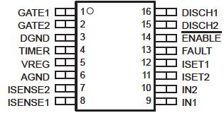
Features: `Dual-Channel High-Side MOSFET Drivers
`IN1: 3 V to 13 V; IN2: 3 V to 5.5 V
`Inrush Current Limiting With dv/dt Control
`Independent Circuit-Breaker Control With Programmable Current Limit and Transient Timer
`CMOS- and TTL-Compatible Enable Input
`Low, 5-mA Standby Supply Current . . . Max
`Available in 16-Pin SOIC and TSSOP Package
`40°C to 85°C Ambient Temperature Range
`Electrostatic Discharge ProtectionApplication·Hot-Swap/Plug/Dock Power Management
·Hot-Plug PCI, Device Bay
·Electronic Circuit BreakerPinout Specifications
Input voltage range: VI(IN1), VI(ISENSE1), VI(ISET1), VI(ENABLE) . . . . . . . . . . . . . . . . . . . . . . . 0.3 V to 15 V
VI(IN2), VI(ISENSE2), VI(ISET2), VI(VREG) . . . . . . . . . . . . . . . . . . . . . . . . . . 0.3 V to 7 V
Output voltage range: VO(GATE1) . . . . . . . . . . . . . . . . . . . . . . . . . . . . . . . . . . . . . . . . . . . . . . . . . 0.3 V to 30 V
VO(GATE2) . . . . . . . . . . . . . . . . . . . . . . . . . . . . . . . . . . . . . . . . . . . . . . . . . . 0.3 V to 22V
VO(DISCH1), VO(FAULT), VO(DISCH2), VO(TIMER), . . . . . . . . . . . . . . . 0.3 V to 15V
Sink current range: IGATE1, IGATE2, IDISCH1, IDISCH2 . . . . . . . . . . . . . . . . . . . . . . . . . . . . . . 0 mA to 100 mA
ITIMER, IFAULT . . . . . . . . . . . . . . . . . . . . . . . . . . . . . . . . . . . . . . . . . . . . . . . . 0 mA to 10 mA
Operating virtual junction temperature range, TJ . . . . . . . . . . . . . . . . . . . . . . . . . . . . . . . . . . . . . 40°C to 100°C
Storage temperature range, Tstg . . . . . . . . . . . . . . . . . . . . . . . . . . . . . . . . . . . . . . . . . . . . . . . . . . . 55°C to 150°C
Lead temperature 1,6 mm (1/16 inch) from case for 10 seconds . . . . . . . . . . . . . . . . . . . . . . . . . . . . . . . 260°C
† Stresses beyond those listed under "absolute maximum ratings" may cause permanent damage to the device. These are stress ratings only, and functional operation of the device at these or any other conditions beyond those indicated under "recommended operating conditions" is not implied. Exposure to absolute-maximum-rated conditions for extended periods may affect device reliability.
NOTE 1: All voltages are respect to DGND.
DescriptionThe TPS2320 and TPS2321 are dual-channel hot-swap controllers that use external N-channel MOSFETs as high-side switches in power applications. Features of these devices, such as overcurrent protection (OCP), inrush-current control, and separation of load transients from actual load increases, are critical requirements for hot-swap applications.
The TPS2320 and TPS2321 devices incorporate undervoltage lockout (UVLO) to ensure the device is off at startup. Each internal charge pump, capable of driving multiple MOSFETs, provides enough gate-drive voltage to fully enhance the N-channel MOSFETs. The charge pumps control both the rise times and fall times (dv/dt) of the MOSFETs, reducing power transients during power up/down. The circuit-breaker functionality combines the ability to sense overcurrent conditions with a timer function; this allows designs such as DSPs, that may have high peak currents during power-state transitions, to disregard transients for a programmable period.

 TPS2320 Data Sheet


