TPS2102

Features: Dual-Input, Single-Output MOSFET Switch With No Reverse Current Flow (No Parasitic Diodes)IN1 . . . 250-W, 500-mA N-Channel; 16-mA Max Supply CurrentIN2 . . . 1.3-, 10-A P-Channel; 1.5-mA Max Supply Current (VAUX Mode)Advanced Switch Control LogicCMOS- and TTL-Compatible Enable InputCont...

product image

TPS2102 Picture
SeekIC No. : 004526556 Detail

TPS2102: Features: Dual-Input, Single-Output MOSFET Switch With No Reverse Current Flow (No Parasitic Diodes)IN1 . . . 250-W, 500-mA N-Channel; 16-mA Max Supply CurrentIN2 . . . 1.3-, 10-A P-Channel; 1.5-mA ...

floor Price/Ceiling Price

Part Number:
TPS2102
Supply Ability:
5000

Price Break

  • Qty
  • 1~5000
  • Unit Price
  • Negotiable
  • Processing time
  • 15 Days
Total Cost: $ 0.00

SeekIC Buyer Protection PLUS - newly updated for 2013!

  • Escrow Protection.
  • Guaranteed refunds.
  • Secure payments.
  • Learn more >>

Month Sales

268 Transactions

Rating

evaluate  (4.8 stars)

Upload time: 2025/1/11

Payment Methods

All payment methods are secure and covered by SeekIC Buyer Protection PLUS.

Notice: When you place an order, your payment is made to SeekIC and not to your seller. SeekIC only pays the seller after confirming you have received your order. We will also never share your payment details with your seller.
Product Details

Description


Features:

 Dual-Input, Single-Output MOSFET Switch With No Reverse Current Flow (No Parasitic Diodes)
 IN1 . . . 250-W, 500-mA N-Channel; 16-mA Max Supply Current
 IN2 . . . 1.3-, 10-A P-Channel; 1.5-mA Max Supply Current (VAUX Mode)
 Advanced Switch Control Logic
 CMOS- and TTL-Compatible Enable Input
 Controlled Rise, Fall, and Transition Times
 2.7-V to 4 V Operating Range
 SOT-23-5 and SOIC-8 Package
 40°C to 70°C Ambient Temperature Range
2-kV Human-Body-Model, 750-V CDM, 200-V Machine-Model Electrostatic- Discharge Protection


Application

 Notebook and Desktop PCs
 Cell phone, Palmtops, and PDAs
 Battery Management


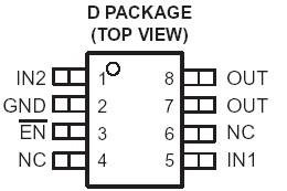
Pinout

  Connection Diagram


Specifications

Input voltage range, VI(IN1) (see Note1) . . . . . . . . . . . . . . . . . . . . . . . . . . . . . . . . . .0.3 V to 5 V
Input voltage range, VI(IN2) (see Note1) . . . . . . . . . . . . . . . . . . . . . . . . . . . . . . . . . .0.3 V to 5 V
Input voltage range, VI at EN or EN (see Note 1) . . . . . . . . . . . . . . . . .. . . . . . . . . . .0.3 V to 5 V
Output voltage range, VO (see Note 1) . . . . . . . . . . . . . . . . . . . . . . . . . . . . . . . . . . .0.3 V to 5 V
Continuous output current, IO(IN1)  . . . . . . . . . . . . . . . . . . . . . . . . . . . . . . . . . . . . . . . . . .700 mA
Continuous output current, IO(IN2)  . . . . . . . . . . . . . . . . . . . . . . . . . . . . . . . . . . . . . . . . .  .140 mA
Continuous total power dissipation  . . . . . . . . . . . . . . . . . . . . . . . . . .See dissipation rating table
Operating virtual junction temperature range, T . . . . . . . . . . . . . . . .  . . . . . . . . .40°C to 85°C
Storage temperature range, Tstg  . . . . . . . . . . . . . . . . . . . . . . . . . . . . . . . . . . . . 65°C to 150°C
Lead temperature soldering 1,6 mm (1/16 inch) from case for 10 seconds  .  . . . . . . . . . . .260°C
Electrostatic discharge (ESD) protection: Human body model  . . . . . . . . . . . . . . . .  . . . . . . . .2 kV
                                                                Machine model  . . . . . . . . . . . . . . . . . . .. . . . . . . .200 V
                                                                Charged device model (CDM)  . . . . . . . . .  . . . . . .750 V


Description

The TPS2102 and TPS2103 are dual-input, single-output power switches designed to provide uninterrupted output voltage when transitioning between two independent power supplies. Both devices combine one n-channel (250 m) and one p-channel (1.3 ) MOSFET with a single output. The p-channel MOSFET (IN2) is used with auxiliary power supplies that deliver lower current for standby modes. The n-channel MOSFET (IN1) is used with a main power supply that delivers higher current required for normal operation. Low on-resistance makes the n-channel the ideal path for higher main supply current when power-supply regulation and system voltage drops are critical. When using the p-channel MOSFET, quiescent current is reduced to 0.75 A to decrease the demand on the standby power supply. The MOSFETs in the TPS2102 and TPS2103 do not have the parasitic diodes, found in discrete MOSFETs, which allow the devices to prevent back-flow current when the switch is off.


Customers Who Bought This Item Also Bought

Margin,quality,low-cost products with low minimum orders. Secure your online payments with SeekIC Buyer Protection.
Optical Inspection Equipment
Potentiometers, Variable Resistors
Programmers, Development Systems
Prototyping Products
DE1
Fans, Thermal Management
Audio Products
View more