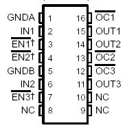
Features: 80-mΩ High-Side MOSFET Switch
250 mA Continuous Current Per Channel
Independent Thermal and Short-Circuit Protection With Overcurrent Logic Output
Operating Range . . . 2.7 V to 5.5 V
CMOS- and TTL-Compatible Enable Inputs
2.5-ms Typical Rise Time
Undervoltage Lockout
10 µA Maximum Standby Supply Current for Single and Dual (20 µA for Triple and Quad)
Bidirectional Switch
Ambient Temperature Range, 0°C to 85°C
ESD Protection
ApplicationAudio
Automotive
Broadband
Digital Control
Military
Optical Networking
Security
Telephony
Video & Imaging
WirelessPinout SpecificationsInput voltage range, VI(IN) (see Note 1). . . . . . . . . . . . . . . . . . . . . . . . . . . . . . . . . . . . . . 0.3 V to 6 V
Output voltage range, VO(OUT) (see Note 1) . . . . . . . . . . . .. . . . . . . . . . . . . . .0.3 V to VI(IN) + 0.3 V
Input voltage range, VI(ENx) or VI(ENx) . . . . . . . . . . . . . . . . . . . . . . . . . . . . . . . . . . . . . .0.3 V to 6 V
Continuous output current, IO(OUT) . . . . . . . . . . . . . . . . . . . . . . . . . . . . . . . . . . . . . . .internally limited
Continuous total power dissipation . . . . . . . . . . . . . . . . . . . . . . . . . . . . . . .See Dissipation Rating Table
Operating virtual junction temperature range, TJ . . . . . . . . . . . . . . . . . . . . . . . . . . . . . . 0°C to 125°C
Storage temperature range, Tstg . . . . . . . . . . . . . . . . . . . . . . . . . . . . . . . . . . . . . . . . 65°C to 150°C
Lead temperature soldering 1,6 mm (1/16 inch) from case for 10 seconds . . . . . . . . . . . . . . . .. . 260°C
Electrostatic discharge (ESD) protection: Human body model MIL-STD-883C . . . . . . . . . . . . . . . . . .2 kV
Machine model . . . . . . . . . . . . . . . . . . . . .. . . . . . . . .0.2 kV DescriptionThe TPS2045A, TPS2048A and TPS2055A , TPS2058A power-distribution switches are intended for applications where
heavy capacitive loads and short circuits are likely to be encountered. These TPS2045A, TPS2048A and TPS2055A , TPS2058A devices incorporate 80-mΩ N-channel MOSFET high-side power switches for power-distribution systems that require multiple power switches in a single package. Each switch is controlled by an independent logic enable input. Gate drive is provided by an internal charge pump designed to control the power-switch rise times and fall times to minimize current surges during switching. The charge pump requires no external components and allows operation from supplies as low as 2.7 V.
When the output load of TPS2045A, TPS2048A and TPS2055A , TPS2058A exceeds the current-limit threshold or a short is present, these devices limit the output current to a safe level by switching into a constant-current mode, pulling the overcurrent (OCx) logic output low. When continuous heavy overloads and short circuits increase the power dissipation in the switch, causing the junction temperature to rise, a thermal protection circuit shuts off the switch to prevent damage. Recovery from a thermal shutdown is automatic once the device has cooled sufficiently. Internal circuitry ensures the switch remains off until valid input voltage is present. These TPS2045A, TPS2048A and TPS2055A , TPS2058A power-distribution switches are designed to current limit at 0.5 A.

 TPS2047A Data Sheet


