TPIC6259

Features: • Low rDS(on) . . . 1.3 W Typical• Avalanche Energy . . . 75 mJ• Eight Power DMOS Transistor Outputs of 250-mA Continuous Current• 1.5-A Pulsed Current Per Output• Output Clamp Voltage at 45 V• Four Distinct Function Modes• Low Power ConsumptionP...

product image

TPIC6259 Picture
SeekIC No. : 004526396 Detail

TPIC6259: Features: • Low rDS(on) . . . 1.3 W Typical• Avalanche Energy . . . 75 mJ• Eight Power DMOS Transistor Outputs of 250-mA Continuous Current• 1.5-A Pulsed Current Per Output&#...

floor Price/Ceiling Price

Part Number:
TPIC6259
Supply Ability:
5000

Price Break

  • Qty
  • 1~5000
  • Unit Price
  • Negotiable
  • Processing time
  • 15 Days
Total Cost: $ 0.00

SeekIC Buyer Protection PLUS - newly updated for 2013!

  • Escrow Protection.
  • Guaranteed refunds.
  • Secure payments.
  • Learn more >>

Month Sales

268 Transactions

Rating

evaluate  (4.8 stars)

Upload time: 2025/1/11

Payment Methods

All payment methods are secure and covered by SeekIC Buyer Protection PLUS.

Notice: When you place an order, your payment is made to SeekIC and not to your seller. SeekIC only pays the seller after confirming you have received your order. We will also never share your payment details with your seller.
Product Details

Description


Features:

• Low rDS(on) . . . 1.3 W Typical
• Avalanche Energy . . . 75 mJ
• Eight Power DMOS Transistor Outputs of 250-mA Continuous Current
• 1.5-A Pulsed Current Per Output
• Output Clamp Voltage at 45 V
• Four Distinct Function Modes
• Low Power Consumption


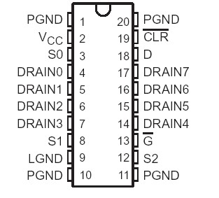
Pinout

  Connection Diagram


Specifications

Logic supply voltage, VCC (see Note 1). . . . . . . . . . . . . . . . .  . . . . . . . . . . . . . . . . . . . . . . . 7 V
Logic input voltage range, VI . . . . . . . . . . . . . . . . . . . . . . . . . . . . . . .. . . . . . . . . .0.3 V to 7 V
Power DMOS drain-to-source voltage, VDS (see Note 2) . . . . . . . . . . . . . . . . . . . . . . . . . .45 V
Continuous source-drain diode anode current . . . . . . . . . . . . . . . . . . . . . . . . . . . . . . . . . . 1 A
Pulsed source-drain diode anode current . . . . . . . . . . . . . . . . . . . . . . . . . . . . . . . .. . . . . . 2 A
Pulsed drain current, each output, all outputs on, IDn, TA = 25°C (see Note 3) . . . . . .750 mA
Continuous drain current, each output, all outputs on, IDn, TA = 25°C . . . . . . . . . . . . 250 mA
Peak drain current single output, IDM, TA = 25°C (see Note 3) . . . . . . .. . . . .  . . . . . . . . . .2 A
Single-pulse avalanche energy, EAS (see Note 4) . . . . . . . . . . . . . . . . . . . . . . . .. . . . . . 75 mJ
Avalanche current, IAS (see Note 4) . . . . . . . . . . . . . . . . . . . . . . . . . . . . . . . . . . . . . . . . . . 1 A
Continuous total power dissipation . . . . . . . . . . . . . . . .. . . . . . . See Dissipation Rating Table
Operating virtual junction temperature range, TJ . . . . . . . . . . . . . . . . . . . . .  .40°C to 150°C
Storage temperature range, Tstg . . . . . . . . . . . . . . . . . . . . . . . . . . . . . . . . . . 65°C to 150°C
Lead temperature 1.6 mm (1/16 inch) from case for 10 seconds . . . . . . .. . . . . . . . . . . . 60°C


Description

This TPIC6259 power logic 8-bit addressable latch controls open-drain DMOS transistor outputs and is designed for general-purpose storage applications in digital systems. Specific uses include working registers, serial-holding registers, and decoders or demultiplexers. This is a multifunctional device capable of storing single-line data in eight addressable latches with 3-to-8 decoding or demultiplexing mode active-low DMOS outputs.

Four distinct modes of operation are selectable by controlling the clear (CLR) and enable (G) inputs as enumerated in the function table. In the addressable-latch mode, data at the data-in (D) terminal is written into the addressed latch. The addressed DMOS transistor output inverts the data input with all unaddressed DMOS-transistor outputs remaining in their previous states. In the memory mode, all DMOS-transistor outputs remain in their previous states and are unaffected by the data or address inputs. To eliminate the possibility of entering erroneous data in the TPIC6259 latch, enable G should be held high (inactive) while the address lines are changing. In the 3-to-8 decodingor demultiplexing mode, the addressed output is inverted with respect to the D input and all other outputs are high. In the clear mode, all outputs are high and unaffected by the address and data inputs.

Separate power and logic level ground pins are provided to facilitate maximum system flexibility. Pins 1, 10, 11, and 20 are internally connected, and each pin of TPIC6259 must be externally connected to the power system ground in order to minimize parasitic inductance. A single-point connection between pin 9, logic ground (LGND), and pins 1, 10, 11, and 20, power ground (PGND) must be externally made in a manner that reduces crosstalk between the logic and load circuits.

The TPIC6259 is characterized for operation over the operating case temperature range of 40°C to 125°C.


Customers Who Bought This Item Also Bought

Margin,quality,low-cost products with low minimum orders. Secure your online payments with SeekIC Buyer Protection.
Crystals and Oscillators
Cables, Wires
Integrated Circuits (ICs)
Static Control, ESD, Clean Room Products
Semiconductor Modules
View more