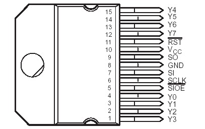
Pinout Specifications
Supply voltage range, VCC (see Note 1) . . . . . . . . . . . . . . . . . . . . . . . . . . . . . . . 0.3 V to 7 V
Input voltage, VI . . . . . . . . . . . . . . . . . . . . . . . . . . . . . . . . . . . . . . . . . . . . . . . . . . . . .. .. . . 7 V
Output voltage range, SO . . . . . . . . . . . . . . . . . . . . . . . . . . . . . . . . . . . . . . . . .. . 0.3 V to 7 V
Input current, II . . . . . . . . . . . . . . . . . . . . . . . . . . . . . . . . . . . . . . . . . . . . . . . . . . . . . . .15 mA
Peak output sink current at Y, IO repetitive, tw = 10 ms, duty cycle = 50%,
(see Notes 2 and 3). . . . . . . . . . . . . . . . . . . . . . . . . . . . . . . . . . . . . . . . . . . . . internally limited
Continuous output current at Y, IO (see Note 3) . . . . . . . . . . . . . . . . . . . . . . . . . . . . . . . . . .1 A
Peak current through GND terminal: Nonrepetitive tw = 0.2 ms . . . . . . . . . . . . . . . . . . . . .. 8 A
Repetitive tw = 10 ms, duty cycle = 50% . . . . . . . . . . . . . . . . .. . . . 6 A
Continuous current through GND terminal . . . . . . . . . . . . . . . . . . . . . . . . . . . . . .. . . . . . 4.5 A
Single-pulse avalanche energy rating, EAS (see Note 4) . . . . . . . . . . . . . . . . . . . . . . . . . . .20 mJ
Avalanche current, IAS(max) (see Note 5) . . . . . . . . . . . . . . . . . . . . . . . . . . . . . . .. . . . . . . . .1 A
Continuous dissipation at (or below) TA = 25 (see Note 6) . . . . . . . . . . . . . . . . . .. . . 3.575 W
Continuous dissipation at (or below) TC = 75 (see Note 6) . . . . . . . . . . . . . . . . . . . . . . . 25 W
Operating case or virtual-junction temperature range . . . . . . . . . . . . . . . . . . . . 55 to 150
Storage temperature range, Tstg . . . . . . . . . . . . . . . . . . . . . . . . . . . . . . . . . . . .. 65 to 150
Lead temperature 1,6 mm (1/16 inch) from case for 10 seconds . . . . . . . . . . . . . . . . . . . . . .260
NOTES:
1. All voltage values are with respect to network GND.
2. Each Y output is individually current limited with a typical overcurrent limit of about 1.8 A.
3. Multiple Y outputs of this device can conduct rated current simultaneously; however, power dissipation (average) over a short time
interval must fall within the continuous dissipation range and the GND terminal current range.
4. VCC = 20 V, starting TJ = 25°C, L = 310 mH, IAS = 0.28 A.
5. VCC = 10 V, starting TJ = 25°C, L = 8 mH, IAS = 1 A (see Figure 6).
6. For operation above 25°C free-air temperature, derate linearly at the rate of 28.6 mW/°C. For operation above 75°C case
temperature, derate linearly at the rate of 333 mW/°C. To avoid exceeding the maximum virtual-junction temperature, these ratings
must not be exceeded.
DescriptionThe TPIC2802 octal intelligent-power switch is a monolithic BIDFET† integrated circuit designed to sink currents up to 1 A at 45 V simultaneously at each of eight driver outputs under serial input data control. Furthermore, use of a Darlington output structure enables an 80% reduction in the on-state supply current compared with earlier designs. Status of the individual driver outputs is available in serial data format. The TPIC2802 driver outputs have overcurrent limiting and out-of-saturation voltage protection features. Applications of TPIC2802 include driving solenoids, relays, dc motors, lamps, and other medium-current or high-voltage loads.
The TPIC2802 device contains an 8-bit serial-in, parallel-out shift register that feeds an 8-bit parallel latch, which independently controls each of the eight Y-output drivers.
Data of TPIC2802 is entered into the device serially via the serial input (SI) and goes directly into the lowest bit (0) of the shift register. Using proper timing signals, the input data is passed to the corresponding output latch and output driver. A logic-high SI bit n turns the corresponding output driver (Yn)off. A logic-low bit at SI turns the corresponding output driver on. Serial data is transferred into SI on the high-to-low transition of the serial clock (SCLK) input in 8-bit bytes with data for the Y7 output (most significant bit) first and data for Y0 output (least significant bit) last. Both SI and SCLK are active when the serial input-output enable (SIOE) input is low and are disabled when SIOE is high.
Each TPIC2802 driver output is monitored by a voltage comparator that compares the Y-output voltage level with an internal out-of-saturation threshold voltage reference level. The logic state of the comparator output is dependent upon whether the Y output is greater or smaller than the reference voltage level. While SIOE is held high, an activated driver output is unlatched and turned off when the output voltage exceeds the out-of-saturation threshold voltage level except when the internal unlatch enable is low and disabled. The high-to-low transition of SIOE transfers the logic state of the comparator output to the shift register.

 TPIC2802 Data Sheet


