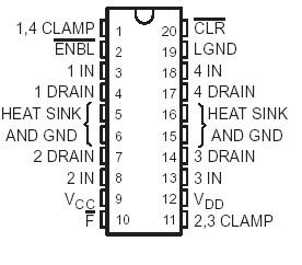
Pinout Specifications
Logic supply voltage, VCC (see Note 1) . . . . . . . . . . . . . . . . . . . . . . . . . . . . . . . . . .. . . . . . . . .7 V
Power MOSFET driver supply voltage, VDD . . . . . . . . . . . . . . . . . . . . . . . . . . . . . . . . . . . . . . . .60 V
Logic input voltage, VI . . . . . . . . . . . . . . . . . . . . . . . . . . . . . . . . . . . . . . . . . . . . . . . . . . . . . . . .7 V
Power MOSFET drain-source voltage, VDS . . . . . . . . . . . . . . . . . . . . . . . . . . .. . . . . . . . . . . . . .60 V
Output voltage at F, VO . . . . . . . . . . . . . . . . . . . . . . . . . . . . . . . . . . . . .. . . . . . . . . . . . . . . . . . .7 V
Clamp-diode voltage . . . . . . . . . . . . . . . . . . . . . . . . . . . . . . . . . . . . . . . . . . . . . . . . . . . . . . . . .60 V
Continuous source-drain diode anode current . . . . . . . . . . . . . . . . . . . . . . . . . . . . . . . . . .. .1.25 A
Pulsed source-drain diode anode current . . . . . . . . . . . . . . . . . . . . . . . . . . . . . . . . . . . . . . . . . .6 A
Pulsed drain current, each output, all outputs on, ID1 = ID2 = ID3 = ID4, TA = 25
(see Note 2 and Figures 5 through 8) . . . . . . . . . . . . . . . . . . . . . . . . . . . . . . . . . . . . . . . . . . . . .3 A
Continuous drain current, each output, all outputs on, ID1 = ID2 = ID3 = ID4, TA = 25 .. .. .770 mA
Peak drain current, single output, IDM, TA = 25 (see Note 3) . . . . . . . . . . . . . . . . . . . . . . . .12.5 A
Single-pulse avalanche energy, EAS. . . . . . . . . . . . . . . . . . . . . . . . . . . . . . . . . . .. . . . . . . . . . . 50 mJ
Continuous total dissipation at or below 25 free-air temperature (see Note 4) . . . . . . . . . .2.5 W
Continuous total dissipation at or below 100°C case temperature (see Note 4 . . . . . . . . . . . . .6 W
Operating junction temperature range, TJ . . . . . . . . . . . . . . . . . . . . . . . . . . . . . . . .40 to 150
Storage temperature range . . . . . . . . . . . . . . . . . . . . . . . . . . . . . . . . . . . . . . . . . . .40 to 150
Lead temperature 1.6 mm (1/16 inch) from case for 10 seconds . . . . . . . . . . . . . . . . . . . . . . . 260
NOTES: 1. All voltage values are with respect to the five ground (GND and LGND) terminals connected together.
2. Pulse duration = 10 ms, duty cycle = 6%.
3. Pulse duration 3 100 ms, duty cycle 3 2%.
4. For operation above 25°C free-air temperature, derate linearly at the rate of 20 mW/°C. For operation above 100°C case temperature,
derate linearly at the rate of 120 mW/°C. To avoid exceeding the design maximum junction temperature, these ratings should not be
exceeded. Due to variations in individual devices, electrical characteristics, and thermal resistance, the built-in thermal overload
protection can be activated at power levels slightly above or below the rated dissipation.
DescriptionThe TPIC2406 is a monolithic, high-voltage,high-current, quadruple power driver designed foruse in systems that require high load power. The TPIC2406 device contains built-in high-speed output clamp diodes for inductive transient protection. Power driver applications include lamps, relays, solenoids, and dc stepping motors.
The TPIC2406 device features four inverting open-drain outputs, each controlled by an input storage latch with common clear and enable controls. All inputs accept standard TTL- and CMOS-logic levels. The CLR function is asynchronous and turns all four outputs off regardless of data inputs. Taking ENBL low puts the input latch into a transparent mode, allowing the data inputs to affect the output. In this state, all four outputs are held off while CLR is low, but return to the stages on the data inputs when CLR goes high. When ENBL is taken high, the latch is put into a storage mode and the last state of the data inputs is held in the latches. If CLR is taken low, the data in the latches is cleared and all outputs are turned off. If CLR is taken high again, ENBL must be cycled low to read new data into the latch.

 TPIC2406 Data Sheet


