TPIC1533

Features: Low rDS(on): 0.1 Typ (Full H-Bridge) 0.22 Typ (Triple Half H-Bridge)Pulsed Current:12 A Per Channel (Full H-Bridge)6 A Per Channel (Triple Half H-Bridge)Matched Sense Transistor for Class A-B Linear OperationFast Commutation SpeedPinoutSpecificationsSupply-to-GND voltage . . . . . . . ....

product image

TPIC1533 Picture
SeekIC No. : 004526353 Detail

TPIC1533: Features: Low rDS(on): 0.1 Typ (Full H-Bridge) 0.22 Typ (Triple Half H-Bridge)Pulsed Current:12 A Per Channel (Full H-Bridge)6 A Per Channel (Triple Half H-Bridge)Matched Sense Transistor for Class...

floor Price/Ceiling Price

Part Number:
TPIC1533
Supply Ability:
5000

Price Break

  • Qty
  • 1~5000
  • Unit Price
  • Negotiable
  • Processing time
  • 15 Days
Total Cost: $ 0.00

SeekIC Buyer Protection PLUS - newly updated for 2013!

  • Escrow Protection.
  • Guaranteed refunds.
  • Secure payments.
  • Learn more >>

Month Sales

268 Transactions

Rating

evaluate  (4.8 stars)

Upload time: 2025/1/11

Payment Methods

All payment methods are secure and covered by SeekIC Buyer Protection PLUS.

Notice: When you place an order, your payment is made to SeekIC and not to your seller. SeekIC only pays the seller after confirming you have received your order. We will also never share your payment details with your seller.
Product Details

Description


Features:

 Low rDS(on): 0.1 Typ (Full H-Bridge) 0.22 Typ (Triple Half H-Bridge)
 Pulsed Current: 12 A Per Channel (Full H-Bridge) 6 A Per Channel (Triple Half H-Bridge)
 Matched Sense Transistor for Class A-B Linear Operation
 Fast Commutation Speed


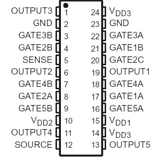
Pinout

  Connection Diagram


Specifications

Supply-to-GND voltage . . . . . . . . . . . . . . . . . . . . . . . . . . . . . . . . . . . . . . . . . . . . . . . . . . . . . . . . .  .20 V
Source-to-GND voltage (Q3A, Q4A, Q5A)  . . . . . . . . . . . . . . . . . . . . . . . . . . . . . . . . . . . . . . . . .. . . .20 V
Output-to-GND voltage  . . . . . . . . . . . . . . . . . . . . . . . . . . . . . . . . . . . . . . . . . . . . . . . . . . . . . . . . . .20 V
Sense-to-GND voltage  . . . . . . . . . . . . . . . . . . . . . . . . . . . . . . . . . . . . . . . . . . . . . . .. . . . . . . . . . . .20 V
Gate-to-source voltage range, VGS (Q1A, Q1B, Q2A, Q2B) . . .. .  . . . . . . . . . . . . . . . . . . . . . . . . . ±20 V
Gate-to-source voltage range, VGS (Q3A, Q3B, Q4A, Q4B, Q5A, Q5B)  . . . . . . . . . . . . . . .0.3 V to 20 V

Gate-to-source voltage range, VGS (Q2C) . . . . . . . . . . . . . . . . . . . . . . . . . . . . . . . . . . . .  .0.7 V to 6 V
Continuous gate-to-source zener-diode current (Q2C)  . . . . . . . . . . . . . . . . . . . . . . . . . . . . . . .±10 mA
Pulsed gate-to-source zener-diode current (Q2C)  . . . . . . . . . . . . . . . . . . . . . . . . . . . . . .  . . . .±50 mA

Continuous drain current, each output (Q1A, Q1B, Q2A, Q2B) . . . . . . . . . . . . . . . . . . . . . . . .  . .   . .3A
Continuous drain current, each output (Q3A, Q3B, Q4A, Q4B, Q5A, Q5B)  . . . . . . . . . . . . .. . . . . . 1.5 A
Continuous drain current (Q2C)  . . . . . . . . . . . . . . . . . . . . . . . . . . . . . . . . . . . . . . . . . . . .  . . . . . .15 mA
Continuous source-to-drain diode current (Q1A, Q1B, Q2A, Q2B)  . . . . . . . . . . . . . . . . . . . .  . . . .   .3A
Continuous source-to-drain diode current (Q3A, Q3B, Q4A, Q4B, Q5A, Q5B) . . . . . . . . . . . . . . . . . 1.5 A
Continuous source-to-drain diode current (Q2C)  . . . . . . . . . . . . . . . . . . . . . . . . . . . . . . . . . . . . . 15 mA
Pulsed drain current, each output, Imax (Q1A, Q1B, Q2A, Q2B) (see Note 1 and Figure 24)  . . .. .  .12A
Pulsed drain current, each output, Imax (Q3A, Q3B, Q4A, Q4B, Q5A, Q5B)
                 (see Note 1 and Figure 25). . . . . . . . .  . . . . . . . . . . . . . . . . . . . . . . . . . . . . . . . .  . . .    6 A
Pulsed drain current, Imax (Q2C) (see Note 1)  . . . . . . . . . . . . . . . . . . . . . . . . . . . . . . .  . . . . . . .60 mA
Continuous total power dissipation, TC = 70°C (see Note 2 and Figures 24 and 25)  . . . .   .. . .2.86 W
Operating virtual junction temperature range, TJ  . . . . . . . . . . . . . . . . . . . . . . . . . .. . .40°C to 150°C
Operating case temperature range, T . . . . . . . . . . . . . . . . . . . . . . . . . . . . . .. . . . . . .40°C to 125°C
Storage temperature range, Tstg . . . . . . . . . . . . . . . . . . . . . . . . . . . . . . . . . . . . . .. . . .65°C to 150°C
Lead temperature 1,6 mm (1/16 inch) from case for 10 seconds  . . . . . . . . . . . . . . . . . .  . . . . . .260°C


Description

The TPIC1533 is a monolithic power DMOS array that consists of ten electrically isolated N-channel enhancement-mode power DMOS transistors, four of which are configured as a full H-bridge and six as a triple half H-bridge. The lower stage of the full H-bridge is provided with an integratedsense-FET to allow biasing of the bridge in class A-B operation.

The TPIC1533 is offered in a 24-pin wide-body surface-mount (DW) package and is characterized for operation over the case temperature range of 40°C to 125°C. 


Customers Who Bought This Item Also Bought

Margin,quality,low-cost products with low minimum orders. Secure your online payments with SeekIC Buyer Protection.
Programmers, Development Systems
Inductors, Coils, Chokes
RF and RFID
Batteries, Chargers, Holders
Integrated Circuits (ICs)
Power Supplies - External/Internal (Off-Board)
View more