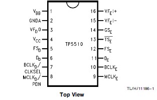
Features: `Complete A/D and D/A with filter system including:`Serial Data Interface`Encode high-pass and low-pass filter`Decode low-pass filter with sin x/x correction`Active RC noise filters`-law compatible A/D and D/A`Internal precision voltage reference`Internal auto-zero circuitry`-lawÐTP5...
TP5510: Features: `Complete A/D and D/A with filter system including:`Serial Data Interface`Encode high-pass and low-pass filter`Decode low-pass filter with sin x/x correction`Active RC noise filters`-law c...
SeekIC Buyer Protection PLUS - newly updated for 2013!
268 Transactions
All payment methods are secure and covered by SeekIC Buyer Protection PLUS.
If Military/Aerospace specified devices are required, please contact the National Semiconductor Sales Office/Distributors for availability and specifications.
VCC to GNDA.............. 7V
VBB to GNDA ................-7V
Voltage at any Analog Input
or Output........................VCC+0.3V to VBB-0.3V
Voltage at any Digital Input or
Output........................VCC+0.3V to GNDA-0.3V
Operating Temperature Range.............. -25°C to a 125°C
Storage Temperature Range............... -65°C to +150°C
Lead Temperature (Soldering, 10 seconds).............. 300°C
ESD (Human Body Model)........................2000V
Latch-Up Immunity = 100 mA on any Pin
The TP5510 consists of a m-law monolithic AFE device utilizingthe A/D and D/A conversion architecture shown in Figure 1 , and a serial data interface. The device is fabricatedusing National's advanced double-poly CMOS process (microCMOS).
The A/D portion of the TP5510 device consists of an input gain adjust amplifier, an active RC pre-filter which eliminates very high frequency noise, and a switched-capacitor band-pass filter that rejects signals below 200 Hz and above 3400 Hz. Also included are auto-zero circuitry and a compressing A/D which samples the filtered signal and converts it to the m-law digital format. The decode portion of the device consists of an expanding D/A, which reconstructs the analog signal from the compressed m-law code, a low-pass filter which corrects for the sin x/x response of the D/A output and rejects signals above 3400 Hz, followed by a singleended power amplifier capable of driving low impedance loads. The device requires a 1.536 MHz, 1.544 MHz or 2.048 MHz master clock, bit clocks which may vary from 64 kHz to 2.048 MHz; and 8 kHz frame sync pulses.