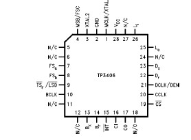
Features: Complete ISDN PBX 2-Wire Data Transceiver including:` 2 B plus D channel interface for PBX UÊ Interface` 144 kb/s full-duplex on 1 twisted pair using Burst Mode` Loop range up to 800 meters (24AWG)` Alternate Mark Inversion coding with transmit filter and scrambler for low emi radi...
TP3406: Features: Complete ISDN PBX 2-Wire Data Transceiver including:` 2 B plus D channel interface for PBX UÊ Interface` 144 kb/s full-duplex on 1 twisted pair using Burst Mode` Loop range up to 800...
SeekIC Buyer Protection PLUS - newly updated for 2013!
268 Transactions
All payment methods are secure and covered by SeekIC Buyer Protection PLUS.
If Military/Aerospace specified devices are required, please contact the National Semiconductor Sales Office/Distributors for availability and specifications.
VCC to GND.............................. 7V
Voltage at Li, Lo ....................VCC+1V to VSS-1V
Voltage at any Digital Input.............. VCC+1V to VSS-1V
Storage Temperature Range............. -65°C to +150°C
Current at Lo......................... ± 100 mA
Current at any Digital Output ..................± 50 mA
Lead Temperature (Soldering, 10 sec.) ..............300°C
ESD (Human Body Model) .....................2000V
The TP3406 is a complete monolithic transceiver for data ransmission on twisted pair subscriber loops. TP3406 is built on ational's double poly microCMOS process, and requires nly a single +5Volt supply. Alternate Mark Inversion (AMI) ine coding, in which binary `1's are alternately transmitted s a positive pulse then a negative pulse, is used to ensure ow error rates in the presence of noise with lower emi radiation han other codes such as Bi-phase (Manchester).
Full-duplex transmission at 144 kb/s is achieved on a single wisted wire pair using a burst-mode technique (Time Compression ultiplexed). Thus the TP3406 device operates as an ISDN U' Interface for short loop applications, typically in a PBX nvironment, providing transmission for 2 B channels and 1 channel. On 24 cable, the range is up to 800 meters.
System timing is based on a Master/Slave configuration, ith the line card end being the Master which controls loop iming and synchronisation. All timing sequences of TP3406 necessary or loop activation and de-activation are generated on-chip. Selection of Master and Slave mode operation is programmed via the Microwire Control Interface.A 2.048 MHz clock, which may be synchronized to the system clock, controls all transmission-related timing functions.