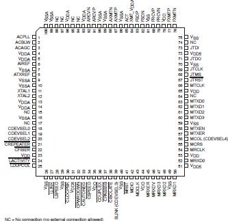
Features: ` Integrated, Single-Chip, Ethernet™ Physical-Layer (PHY) Interface for Full-Duplex or Half-Duplex Connection to 10BASE-T, 100BASE-TX, and 100BASE-FX Networks
` Low-Power 3.3-V CMOS Design With Power-Down Capability for CardBus and Other Applications Requiring Low Power
` Integrated Transmit Filtering and Receive
Equalization Provide for Minimal External
Component Count to Reduce System Cost
` 10BASE-T/100BASE-TX Connection
Supported With Magnetics Package and RJ-45 Connector
` Electrostatic Discharge (ESD) Human Body
Model (HBM) Protection 1.5 kV Per JEDEC
JESD 22-A114-A
` Digital Signal Processor (DSP)-Based
Digital Phase-Locked Loop (PLL)
Technology Allows Data Recovery at 10 Mbit/s and 100 Mbit/s, Requiring One 20-MHz Clock Reference Source
` 10BASE-T
Fully Compliant With IEEE Std 802.3
Smart Squelch for Improved Noise Immunity
Integrated Transmit Wave Shaping
Autopolarity (Reverse-Polarity Correction)
Transmit Jabber Detection
` 100BASE-TX
Fully Compliant With ANSI Twisted-Pair Physical-Media-Dependent (TP-PMD) Standard and IEEE Std 802.3
Synthesized Rise-Time Control
Integrated Receiver With Adaptive Line
Equalization (EQ) and Baseline Wander
(BLW) Correction (DC Restoration)
` IEEE Std 802.3-Compliant
Media-Independent Interface (MII) That
Includes Management Interface
` IEEE Std 802.3-Compliant Autonegotiation
(N-Way) With Next-Page Support
` IEEE Std 1149.1 (JTAG) Test Access Port (TAP)
` Packaged in 100-Terminal Plastic Quad FlatpackPinout Specifications
Supply voltage range: VDD, VDDA, XMT_VDDA, (see Notes 1 and 2)...........0.5 V to 4.6 V
VDD5 (see Notes 1 and 2)......................................0.5 V to 5.5 V
Input voltage range: TTL, VI............................................................0.5 V to VDD + 0.5 V
5-V tolerant TTL, VI......................................0.5 V to VDD5 + 0.5 V
PECL, VI(<4.6 V max) VDD........................... 2.02 V to VDD + 0.5 V
Output voltage range: TTL, VO.........................................................0.5 V to VDD + 0.5 V
5-V tolerant TTL, VO....................................0.5 V to VDD5 + 0.5 V
PECL, VO(<4.6 V max) VDD .........................2.02 V to VDD + 0.5 V
Thermal impedance, junction-to-ambient package, ZJA: Airflow = 068.40°C/W
Airflow = 150 ft/min57.45°C/W
Thermal impedance, junction-to-case package, ZJC...........................................1.95°C/W
Operating case temperature range, TC............................................................0°C to 95°C
Storage temperature range, Tstg................................................................65°C to 150°C
Stresses beyond those listed under "absolute maximum ratings" may cause permanent damage to the device. These are stress ratings only, and functional operation of the device at these or any other conditions beyond those indicated under "recommended operating conditions" is not implied. Exposure to absolute-maximum-rated conditions for extended periods may affect device reliability.
NOTES: 1. All voltage values are with respect to GND.
2. Turning power supplies on and off (cycling sequence) within a mixed 5-V/3.3-V system is an important onsideration. The designer must observe a few rules to avoid damaging the TNETE2101. Check with the anufacturers of all components used in the 3.3-V to 5-V interface to ensure that no unique device characteristics exist that would lead to rules more restrictive than the TNETE2101 requires.
• The optimum solution to power-supply sequencing in a mixed-voltage system is to ramp up the 3.3-V supply first. A power-on reset component operating from this supply forces all 5-V-tolerant outputs into the high-impedance state. Then, the 5-V supply is ramped up. On power down, the 5-V rail deenergizes first, followed by the 3.3-V rail.
• The second-best solution is to ramp both the 3.3-V and the 5-V rails at the same time, making sure that no more than 3.6 V exists between these two rails during the ramp up or down. If the 3.3 V is derived from the 5 V, then the 3.3 V rises as the 5 V rises, so the 5-V rail never exceeds the 3.3-V rail by more than 3.6 V. Both the optimum and second-best algorithms for power up prevent device damage. If it is impractical to implement ramping, follow these rules:
When turning on the power supply, all 3.3-V and 5-V supplies should start ramping from 0 V and reach 95 percent of their end-point values within 25 ms. All bus contention between the device and external devices is eliminated by the end of 25 ms.
When turning off the power supply, 3.3-V and 5-V supplies should start ramping from steady-state values and reach 5 percent of their final values within 25 ms. All bus contention between devices and external devices is eliminated by the end of 25 ms. There is a 250-s lifetime maximum at greater than 3.6-V difference between the supply rails. Holding the ramp-up/ramp-down period to 25 ms per p ower-on/off cycle should not significantly contribute to mean-time-between-failure (MTBF) shifts during product lifetimes.
DescriptionThe TNETE2101 physical-layer (PHY) device from Texas Instruments (TIE) is a single-chip, high-performance solution for a range of 10BASE-T, 100BASE-TX, and 100BASE-FX networking systems (see Figure 1). The highly integrated TNETE2101 includes an on-board media-independent interface (MII) for simple connection to IEEE Std 802.3-compliant media-access controls (MACs). The device integrates all filtering and rise-time control functions for a cost-effective and space-saving PHY solution. Built-in autonegotiation allows automatic selection of half-/full-duplex 10BASE-T or 100BASE-TX, with an autopolarity-correction feature for immunity to receive-pair reversal.

 TNETE2101 Data Sheet


