Features: · SBus Device That Provides Asynchronous Transfer-Mode Interface
· Single-Chip Segmentation and Reassembly (SAR) for Full-Duplex ATM Adaptation- Layer (AAL) Processing
· On-Chip SBus Host Interface Allows Use of Host Memory for Packet SAR
· 53-Byte ATM Cells Are Transparent to the User
· Provides Complete Encapsulation and Termination of AAL5 and Limited AAL3/4
· Features a Null AAL That Provides
Functions for Constant-Bit-Rate Services
· Supports 1023 Unique Virtual Circuits (VCs) on Receive Side
· Explicit Cell-Level Interleaving Between Groups of VCs
· Packet Interface Is Managed by Efficient Descriptor Rings
· Physical (PHY)-Layer Interface Is Full Duplex
· Supports PHY-Layer Data Rates in the Range of 25.6 Mbit/s to 155.52 Mbit/s
· Interfaces Directly to the TNETA1500
SONET ATM BiCMOS Receiver/Transmitter(SABRE)
· Recognizes ATM-Layer Operation and Maintenance (OAM) Cells
· No External Logic Required for Host Bus to Ensure Simple DesignPinout SpecificationsSupply voltage range, VCC (see Note 1) . . . . . . . . . . . . . . . . . . . . . . . . . . 0.5 V to 6 V
Input voltage range, VI . . . . . . . . . . . . . . . . . . . . . . . . . . . . . . . . . 0.5 V to VCC + 0.5 V
Output voltage range, VO . . . . . . . . . . . . . . . . . . . . . . . . . . . . . . . 0.5 V to VCC + 0.5 V
Input clamp current, IIK (VI < 0 or VI > VCC) (see Note 2) . . . . . . . . . . . . . ... . . . ±20 mA
Output clamp current, IOK (VO < 0 or VO > VCC) (see Note 3) . . . . . . . . . .. . . . . . ±20 mA
Operating free air temperature range, TA . . . . . . . . . . . . . . . . . . . . . . . . . . . 0°C to 70°C
Storage temperature range, Tstg . . . . . . . . . . . . . . . . . . . . . . . . . . . . . . . 65°C to 150°C
† Stresses beyond those listed under "absolute maximum ratings" may cause permanent damage to the device. These are stress ratings only, and functional operation of the device at these or any other conditions beyond those indicated under "recommended operating conditions" is not implied. Exposure to absolute-maximum-rated conditions for extended periods may affect device reliability.
NOTES: 1. All voltage values are with respect to the GND terminals.
2. Applies for external input and bidirectional buffers
3. Applies for external output and bidirectional buffersDescriptionThe TNETA1560 is an asynchronous transfer mode (ATM) segmentation and reassembly (SAR) device with an SBus interface. This device incorporates ATM adaptation-layer (AAL) processing, ATM SAR processing for full-duplex operation up to the STS-3c rate of 155.52 Mbit/s, and the controls for the register interface on the physical (PHY) layer. The device provides a packet interface that is managed by descriptor rings, making the 53-byte ATM-framing format transparent to the user. The device passes the payload of 48 bytes, constituting the payload of each cell, across the SBus-host interface. All packets are segmented and reassembled in host memory and accessed by the chip via the descriptor-ring mechanism. This operation reduces the memory requirements for network-interface cards (NICs). The TNETA1560 requires no local processor on the card, which enables very compact solutions.
The applications for the TNETA1560 include NICs for client workstations and servers, embedded applications like LAN emulation, and multiprotocol systems like video servers. The TNETA1560 provides complete AAL5 ncapsulation and termination in hardware. In addition, limited support is provided for AAL3/4 and a null AAL is provided to facilitate real-time data transfer. The TNETA1560 recognizes ATM-layer operation and maintenance (OAM) cells.
In the transmit direction, the TNETA1560 generates data via a special bit-rate control table that provides explicit cell-level interleaving between groups of virtual circuits (VCs). This mechanism brings a higher degree of flexibility hen specifying peak rates for each group (up to 155.52 Mbit/s at a resolution greater than 32 kbit/s). The VCs within a group are serviced via a first-in, first-out (FIFO) discipline on a per-packet basis.
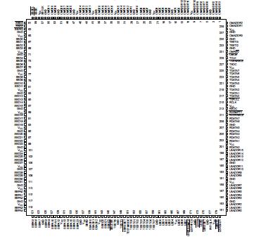
In the receive direction, the TNETA1560 allows multiple virtual paths (VPs) with the condition that each VC is unique. The device is primarily intended for AAL5 encapsulation and termination that is supported in hardware.The TNETA1560 has four interfaces that include: the SBus interface with a 32-bit-wide data bus, the cell interface, a control-memory interface to access the local SRAM, and the local-bus interface to access the PHY-layer register and an EPROM. The cell interface to the PHY layer consists of an 8-bit-wide data path and associated control signals in both the transmit and receive directions. The 53-byte ATM cells pass between the ATM and PHY layers.
The native clock for the TNETA1560 is the SBus clock, which can range between 16.67 MHz and 25 MHz. The native-word size for the device is 32 bits, corresponding to the data width for the SBus. The control-memory interface is 32 bits wide. This interface allows the device to access the local memory to obtain the control information on the packets being segmented and reassembled and to obtain their locations in host memory. Each packet queued for transmission can be distributed across multiple buffers in host memory with each starting at any byte boundary. This is supported in hardware by the device. Every received package is placed in a single buffer in the host memory and is aligned to a 16-byte boundary. The TNETA1560 operation is explained in detail in the Principles of Operation section.

 TNETA1560 Data Sheet


