Operating Supply Voltage
:
Operating Temperature Range
:
Data Bus Width
: 8 bit
On-Chip ADC
: Yes
Mounting Style
: SMD/SMT
Program Memory Size
: 32 KB
Data RAM Size
: 1.5 KB
Maximum Clock Frequency
: 16 MHz
Package / Case
: LQFP
Core
: TLCS-870
Processor Series
: TLCS-870
Features: 1. 8-bit single chip microcomputer TLCS-870/C series
- Instruction execution time :
0.25 s (at 16 MHz)
122 s (at 32.768 kHz)
- 132 types & 731 basic instructions
2. 19interrupt sources (External : 5 Internal : 14)
3. Input / Output ports (39 pins)
Large current output: 4pins (Typ. 20mA), LED direct drive
4. Watchdog Timer
5. Prescaler
- Time base timer
- Divider output function
6. 18-bit Timer/Counter : 1ch
- Timer Mode
- Event Counter Mode
- Pulse Width Measurement Mode
- Frequency Measurement Mode
7. 8-bit timer counter : 4 ch
- Timer, Event counter, Programmable divider output (PDO),
Pulse width modulation (PWM) output,Programmable pulse generation (PPG) modes
8. 8-bit UART/SIO : 1 ch
9. 10-bit successive approximation type AD converter
- Analog input: 8 ch
10. Key-on wakeup : 4 ch
11. LCD driver/controller Built-in voltage booster for LCD driver With display memory
LCD direct drive capability (MAX 32 seg * 4 com) 1/4,1/3,1/2duties or static drive are programmably selectable
12. Clock operation
Single clock mode
Dual clock mode
13. Low power consumption operation STOP mode: Oscillation stops. (Battery/Capacitor back-up.)
SLOW1 mode: Low power consumption operation using low-frequency clock.(High-frequency clock stop.)
SLOW2 mode: Low power consumption operation using low-frequency clock.(High-frequency clock oscillate.)
IDLE0 mode: CPU stops, and only the Time-Based-Timer(TBT) on peripherals operate using high frequency clock. Release by falling edge of the source clock which is set by TBTCR<TBTCK>.
IDLE1 mode: CPU stops and peripherals operate using high frequency clock. Release by interruputs(CPU restarts).
IDLE2 mode: CPU stops and peripherals operate using high and low frequency clock. Release by interruputs.(CPU restarts).
SLEEP0 mode: CPU stops, and only the Time-Based-Timer(TBT) on peripherals operate using low frequency clock.Release by falling edge of the source clock which is set by TBTCR<TBTCK>.
SLEEP1 mode: CPU stops, and peripherals operate using low frequency clock. Release by interruput.(CPU restarts).
SLEEP2 mode: CPU stops and peripherals operate using high and low frequency clock. Release by interruput.
14.Wide operation voltage:
4.5 V to 5.5 V at 16MHz /32.768 kHz
2.7 V to 5.5 V at 8 MHz /32.768 kHz
1.8 V to 5.5 V at 4.2MHz /32.768 kHz
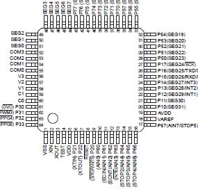
Pinout Specifications
The absolute maximum ratings are rated values which must not be exceeded during operation, even for an instant. Any one of the ratings must not be exceeded. If any absolute maximum rating is exceeded, a device may break down or its performance may be degraded, causing it to catch fire or explode resulting in injury to the user. Thus, when designing products which include this device, ensure that no absolute maximum rating value will ever be exceeded.
| Parameter |
Symbol |
Pins |
Ratings |
Unit |
| Supply voltage |
VDD |
|
−0.3 to 6.5 |
V |
| Input voltage |
VIN |
|
−0.3 to VDD + 0.3 |
V |
| Output voltage |
VOUT1 |
|
−0.3 to VDD + 0.3 |
V |
| Output current (Per 1 pin) |
IOUT1 |
P3, P6 port |
-1.8 |
mA |
| IOUT2 |
P1, P2, P5, P6, P7 port |
3.2 |
| IOUT3 |
P3 port |
30 |
| Output current (Total) |
IOUT2 |
P1, P2, P5, P6, P7 port |
60 |
| IOUT3 |
P3 port |
80 |
| Power dissipation [Topr = 85°C] |
PD |
|
350 |
mW |
| Soldering temperature (Time) |
Tsld |
|
260 (10 s) |
|
| Storage temperature |
Tstg |
|
−55 to 125 |
| Operating temperature |
Topr |
|
−40 to 85 |
DescriptionThe TMP86CM29BUG memory is composed MaskROM, RAM, DBR(Data buffer register) and SFR(Special function register). They are all mapped in 64-Kbyte address space. Figure 2-1 shows the memory address map.

 TMP86CM29BUG Data Sheet


