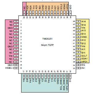
Features: · Compatible with HDMI 1.3a Selection Circuits
· Supports 2.5 Gbps Signaling Rate for 480i/p, 720i/p, and 1080i/p Resolutions up to 12-Bit Color Depth TMDS351 with Port 3 Disabled
· Integrated Switchable Receiver Termination
· Selectable Receiver Equalization toAccommodate to Different Input Cable and Ports 2 and 3 Enabled Lengths
· Intra-Pair Skew < 40 ps Links
· Inter-Pair Skew < 65 ps
· HBM ESD Protection Exceeds 8 kV to TMDS Inputs
· 3.3-V Fixed Supply to TMDS I/Os
· 5-V Fixed Supply to HPD, DDC, and Source Selection Circuits
· 64-Pin TQFP Package
· Footprint Compatible with 3-to-1 Switch
TMDS351 with Port 3 Disabled
· ROHS Compatible and 260°C Reflow Rated
· TMDS250 is Available with Port 1 Disabled and Ports 2 and 3 Enabled
· Supports 5-V to 3.3-V Level Shifting on DDC LinksApplication· Digital TV
· Digital ProjectorPinout Specifications
over operating free-air temperature range (unless otherwise noted)
(1)
| |
UNIT |
| Supply voltage range(2) |
VCC |
0.5 V to 4 V |
| VDD |
0.5 V to 6 V |
| Voltage range |
Anm(3), Bnm |
2.5 V to 4 V |
| Ym, Zm, VSADJ, EQ |
0.5 V to 4 V |
| SCLn, SCL_SINK, SDAn, SDA_SINK, HPDn, HPD_SINK, S1, S2 |
0.5 V to 6 V |
| Electrostatic discharge |
Human body model(4) |
Anm, Bnm, Ym, Zm |
±8000 V |
| All pins |
±4000 V |
| Charged-device model(5) (all pins) |
±1500 V |
| Machine model (6) (all pins) |
±200 V |
| Continuous power dissipation |
See Dissipation Rating Table |
(1) Stresses beyond those listed under absolute maximum ratings may cause permanent damage to the device. These are stress ratings only and functional operation of the device at these or any other conditions beyond those indicated under recommended operating conditions is not implied. Exposure to absolute-maximum-rated conditions for extended periods may affect device reliability.
(2) All voltage values, except differential I/O bus voltages, are with respect to network ground terminal.
(3) n = 1, 2; m = 1, 2, 3, 4
(4) Tested in accordance with JEDEC Standard 22, Test Method A114-B
(5) Tested in accordance with JEDEC Standard 22, Test Method C101-A
(6) Tested in accordance with JEDEC Standard 22, Test Method A115-A
DescriptionThe TMDS251 is a 2-port digital video interface (DVI) or high-definition multimedia interface (HDMI) switch that allows up to 2 DVI or HDMI ports to be switched to a single display terminal. Four TMDS channels, one hot plug detector, and a digital display control (DDC) interface are supported on each port. Each TMDS channel supports signaling rates up to 2.5 Gbps to allow 1080p resolution in 12-bit color depth.
The input port is enabled by configuring source selectors, S1 and S2. When an input port is selected, the TMDS inputs are connected to the TMDS outputs through a 2-to-1 multiplexer, the MOSFET between the input DDC channel and the output DDC channel is turned on, and the HPD output follows the state of the HPD_SINK. The other input port is inactive with disconnected input terminations, disconnected TMDS inputs to the outputs, disconnected DDC inputs to the outputs, and the HPD outputs are low state. Check the source selection look up table for the details of port selections.
When TMDS251 is high and S2 is low, all input terminations are disconnected, TMDS inputs are high impedance with standard TMDS terminations, all internal MOSFETs are turned off to disable the DDC links, and all HPD outputs are connected to the HPD_SINK. This allows the initiation of the HDMI physical address discovery process.
Termination resistors (50-), pulled up to VCC, are integrated at each TMDS receiver input. External terminations are not required. A precision resistor is connected externally from the VSADJ pin to ground for setting the differential output voltage to be compliant with the TMDS standard.
The TMDS251 provides two levels of receiver input equalization for different ranges of cable lengths. Each TMDS receiver owns frequency responsive equalization circuits. When EQ sets low, the receiver supports the input connection in short range HDMI cables. When EQ sets high, the receiver supports the input connection in long range HDMI cables. The TMDS251 supports power saving operation. When a system is under standby mode and there is no digital audio/visual content from a connected source, the 3.3-V supply voltage, VCC, can be powered off to minimize power consumption from the TMDS inputs, outputs, and internal switching circuits. The HPD, DDC, and source selection circuits are powered up by the 5-V supply voltage, VDD, to maintain the system hot plug detect response, the DDC link from the selected source to the sink under system standby operation. The device is characterized for operation from 0°C to 70°C.

 TMDS251 Data Sheet


