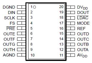
Features: ` Eight Voltage Output DACs in One Package TLV5630 . . . 12-Bit TLV5631 . . . 10-Bit TLV5632 . . . 8-Bit 1 s in Fast Mode 3 s in Slow Mode` Programmable Settling Time vs Power Consumption 1 s in Fast Mode 3 s in Slow Mode 18 mW in Slow Mode at 3 V 48 mW in Fast Mode at 3 V` Compatible Wi...
TLV5631: Features: ` Eight Voltage Output DACs in One Package TLV5630 . . . 12-Bit TLV5631 . . . 10-Bit TLV5632 . . . 8-Bit 1 s in Fast Mode 3 s in Slow Mode` Programmable Settling Time vs Power Consumption ...
SeekIC Buyer Protection PLUS - newly updated for 2013!
268 Transactions
All payment methods are secure and covered by SeekIC Buyer Protection PLUS.
UNIT | |
Supply voltage, (AVDD, DVDD to GND) |
7 V |
Reference input voltage range |
- 0.3 V to AVDD + 0.3 |
Digital input voltage range |
- 0.3 V to DVDD + 0.3 |
Operating free-air temperature range, TA |
-40 to 85 |
Storage temperature range, Tstg |
-65 to 150 |
Lead temperature 1,6 mm (1/16 inch) from case for 10 seconds |
260 |
The TLV5631are pin-compatible, eight-channel, 12-/10-/8-bit voltage output DACs each with a flexible serial interface. The serial interface allows glueless interface to TMS320 and SPI, QSPI, and Microwire serial ports. It is programmed with a 16-bit serial string containing 4 control and 12 data bits.
Additional features of the TLV5631 are a power-down mode, anLDAC input for simultaneous update of all eight DAC outputs, and a data output which can be used to cascade multiple devices, and an internal programmable band-gap reference.
The resistor string output voltage of the TLV5631 is buffered by a rail-to-rail output amplifier with a programmable settling time to allow the designer to optimize speed vs power dissipation. The buffered, high-impedance reference input can be connected to the supply voltage.
Implemented with a CMOS process, the DACs are designed for single-supply operation from 2.7 V to 5.5 V. The devices are available in 20-pin SOIC and TSSOP packages