TLV5614

Features: ` Four 12-Bit D/A Converters` Programmable Settling Time of Either 3 ms or 9 ms Typ` TMS320, (Q)SPI, and Microwire Compatible Serial Interface` Internal Power-On Reset` Low Power Consumption: 8 mW, Slow Mode 5-V Supply 3.6 mW, Slow Mode 3-V Supply` Reference Input Buffer` Voltag...

product image

TLV5614 Picture
SeekIC No. : 004522509 Detail

TLV5614: Features: ` Four 12-Bit D/A Converters` Programmable Settling Time of Either 3 ms or 9 ms Typ` TMS320, (Q)SPI, and Microwire Compatible Serial Interface` Internal Power-On Reset` Low Power Cons...

floor Price/Ceiling Price

Part Number:
TLV5614
Supply Ability:
5000

Price Break

  • Qty
  • 1~5000
  • Unit Price
  • Negotiable
  • Processing time
  • 15 Days
Total Cost: $ 0.00

SeekIC Buyer Protection PLUS - newly updated for 2013!

  • Escrow Protection.
  • Guaranteed refunds.
  • Secure payments.
  • Learn more >>

Month Sales

268 Transactions

Rating

evaluate  (4.8 stars)

Upload time: 2025/1/11

Payment Methods

All payment methods are secure and covered by SeekIC Buyer Protection PLUS.

Notice: When you place an order, your payment is made to SeekIC and not to your seller. SeekIC only pays the seller after confirming you have received your order. We will also never share your payment details with your seller.
Product Details

Description


Features:

` Four 12-Bit D/A Converters
` Programmable Settling Time of Either 3 ms
  or 9 ms Typ
` TMS320, (Q)SPI, and Microwire Compatible
  Serial Interface
` Internal Power-On Reset
` Low Power Consumption:
  8 mW, Slow Mode 5-V Supply
  3.6 mW, Slow Mode 3-V Supply
` Reference Input Buffer
` Voltage Output Range . . . 2* the Reference
  Input Voltage
` Monotonic Over Temperature
` Dual 2.7-V to 5.5-V Supply (Separate Digital
  and Analog Supplies)
` Hardware Power Down (10 nA)
` Software Power Down (10 nA)
` Simultaneous Update


Application

· Battery Powered Test Instruments
· Digital Offset and Gain Adjustment
· Industrial Process Controls
· Machine and Motion Control Devices
· Communications
· Arbitrary Waveform Generation


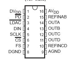
Pinout

  Connection Diagram


Specifications

Supply voltage, (DVDD, AVDD to GND) . . . . . . . . . . . . . . . . . . . . . . . . . . . . . . . . . . . . . . . . . . . . . . . . . . . . . .7 V
Supply voltage difference, (AVDD to DVDD) . . . . . . . . . . . . . . . . . . . . . . . . . . . . . . . . . . . . . . . . .2.8 V to 2.8 V
Digital input voltage range . . . . . . . . . . . . . . . . . . . . . . . . . . . . . . . . . . . . . . . . . . . . . . .0.3 V to DVDD + 0.3 V
Reference input voltage range . . . . . . . . . . . . . . . . . . . . . . . . . . . . . . . . . . . . . . . . . . . .0.3 V to AVDD + 0.3 V
Operating free-air temperature range, TA: TLV5614C . . . . . . . . . . . . . . . . . . . . . . . . . . . . . . . . . . 0°C to 70°C
TLV5614I . . . . . . . . . . . . . . . . . . . . . . . . . . . . . . . . . .  . . . . . . . . . . . . . . . . . . . . . . . . . . . . . . . . 40°C to 85°C
Storage temperature range, Tstg . . . . . . . . . . . . . . . . . . . . . . . . . . . . . . . . . . . . . . . . . . . . . . . 65°C to 150°C
Lead temperature 1,6 mm (1/16 inch) from case for 10 seconds . . . . . . . . . . . . . . . . . . . . . . . . . . . . . . . 260°C


Description

The TLV5614 is a quadruple 12-bit voltage output digital-to-analog converter (DAC) with a flexible 4-wire serial interface. The 4-wire serial interface allows glueless interface to TMS320, SPI, QSPI, and Microwire serial ports. The TLV5614 is programmed with a 16-bit serial word comprised of a DAC address, individual DAC control bits, and a 12-bit DAC value. The device has provision for two supplies: one digital supply for the serial interface (via pins DVDD and DGND), and one for the DACs, reference buffers, and output buffers (via pins AVDD and AGND). Each supply of TLV5614 is independent of the other, and can be any value between 2.7 V and 5.5 V. The dual supplies allow a typical application where the DAC will be controlled via a microprocessor operating on a 3 V supply (also used on pins DVDD and DGND), with the DACs TLV5614 operating on a 5 V supply. Of course, the digital and anlog supplies can be tied together.

The resistor string output voltage of TLV5614  is buffered by a x2 gain rail-to-rail output buffer. The buffer features a Class AB output stage to improve stability and reduce settling time. A rail-to-rail output stage and a power-down mode makes it ideal for single voltage, battery based applications. The settling time of the DAC is programmable to allow the designer to optimize speed versus power dissipation. The settling time of TLV5614 is chosen by the control bits within the 16-bit serial input string. A high-impedance buffer is integrated on the REFINAB and REFINCD terminals to reduce the need for a low source impedance drive to the terminal. REFINAB and REFINCD allo DACs A and B to have a different reference voltage then DACs C and D.

The TLC5614 is implemented with a CMOS process and is available in a 16-terminal SOIC package. The TLV5614C is characterized for operation from 0°C to 70°C. The TLV5614I is characterized for operation from 40°C to 85°C.


Customers Who Bought This Item Also Bought

Margin,quality,low-cost products with low minimum orders. Secure your online payments with SeekIC Buyer Protection.
Boxes, Enclosures, Racks
Memory Cards, Modules
Hardware, Fasteners, Accessories
Soldering, Desoldering, Rework Products
Line Protection, Backups
View more