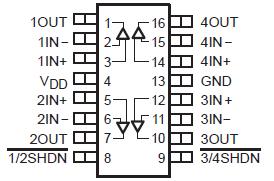
Pinout Specifications
Supply voltage, VDD (see Note 1) . . . . . . . . . . . . . . . . . . . . . . . . . . . . . . . . . . . . . . . . . . . . . . . . . . . . . . . . . 7 V
Differential input voltage, VID (see Note 2) . . . . . . . . . . . . . . . . . . . . . . . . . . . . . . . . . . . . . . . . . . . . . . . . ±VDD
Input voltage range, VI (any input, see Note 1) . . . . . . . . . . . . . . . . . . . . . . . . . . . . . . . . . . . . . . −0.3 V to VDD
Input current, II (any input) . . . . . . . . . . . . . . . . . . . . . . . . . . . . . . . . . . . . . . . . . . . . . . . . . . . . . . . . . . .±4 mA
Output current, IO . . . . . . . . . . . . . . . . . . . . . . . . . . . . . . . . . . . . . . . . . . . . . . . . . . . . . . . . . . . . . . . . . ±50 mA
Total current into VDD+ . . . . . . . . . . . . . . . . . . . . . . . . . . . . . . . . . . . . . . . . . . . . . . . . . . . . . . . . . . . . . ±50 mA
Total current out of GND . . . . . . . . . . . . . . . . . . . . . . . . . . . . . . . . . . . . . . . . . . . . . . . . . . . . . . . . . . . . ±50 mA
Duration of short-circuit current (at or below) 25(see Note 3) . . . . . . . . . . . . . . . . . . . . . . . . . . . . . unlimited
Continuous total power dissipation . . . . . . . . . . . . . . . . . . . . . . . . . . . . . . . . . . . See Dissipation Rating Table
Operating free-air temperature range, TA: Q suffix . . . . . . . . . . . . . . . . . . . . . . . . . . . . . . . . . . . −40to 125
Storage temperature range, Tstg . . . . . . . . . . . . . . . . . . . . . . . . . . . . . . . . . . . . . . . . . . . . . . . . −65to 150
Lead temperature 1,6 mm (1/16 inch) from case for 10 seconds . . . . . . . . . . . . . . . . . . . . . . . . . . . . . . . 260
† Stresses beyond those listed under "absolute maximum ratings" may cause permanent damage to the device. These are stress ratings only, and functional operation of the device at these or any other conditions beyond those indicated under "recommended operating conditions" is not implied. Exposure to absolute-maximum-rated conditions for extended periods may affect device reliability.
NOTES: 1. All voltage values, except differential voltages, are with respect to GND .
2. Differential voltages are at the noninverting input with respect to the inverting input. Excessive current flows when input is brought below GND − 0.3 V.
3. The output may be shorted to either supply. Temperature and/or supply voltages must be limited to ensure that the maximum dissipation rating is not exceeded.
DescriptionThe TLV277x CMOS operational amplifier family combines high slew rate and bandwidth, rail-to-rail output swing, high output drive, and excellent dc-precision. The device provides 10.5 V/s of slew rate and 5.1 MHz of bandwidth while only consuming 1 mA of supply current per channel. This ac-performance is much higher than current competitive CMOS amplifiers. The rail-to-rail output swing and high output drive make these devices a good choice for driving the analog input or reference of analog-to-digital converters. These devices also have low distortion while driving a 600- load for use in telecom systems.
These amplifiers of the TLV277x CMOS have a 360-V input offset voltage, a 17 nV/Hz input noise voltage, and a 2-pA input bias current for measurement, medical, and industrial applications. The TLV277x family is also specified across an extended temperature range (−40 to 125), making it useful for automotive systems.
These devices of the TLV277x CMOS operate from a 2.5-V to 5.5-V single supply voltage and are characterized at 2.7 V and 5 V. The
single-supply operation and low power consumption make these devices a good solution for portable applications. The following table lists the packages available.

 TLV277x CMOS Data Sheet


