TLV2553

Features: 12-Bit-Resolution A/D ConverterUp to 200 KSPS (150 KSPS for 3 V) Throughput Over Operating Temperature Range With 12-Bit Output Mode11 Analog Input Channels3 Built-In Self-Test ModesInherent Sample and Hold FunctionLinearity Error . . . ±1 LSB MaxOn-Chip Conversion ClockUnipolar or Bipol...

product image

TLV2553 Picture
SeekIC No. : 004522364 Detail

TLV2553: Features: 12-Bit-Resolution A/D ConverterUp to 200 KSPS (150 KSPS for 3 V) Throughput Over Operating Temperature Range With 12-Bit Output Mode11 Analog Input Channels3 Built-In Self-Test ModesInhere...

floor Price/Ceiling Price

Part Number:
TLV2553
Supply Ability:
5000

Price Break

  • Qty
  • 1~5000
  • Unit Price
  • Negotiable
  • Processing time
  • 15 Days
Total Cost: $ 0.00

SeekIC Buyer Protection PLUS - newly updated for 2013!

  • Escrow Protection.
  • Guaranteed refunds.
  • Secure payments.
  • Learn more >>

Month Sales

268 Transactions

Rating

evaluate  (4.8 stars)

Upload time: 2025/1/11

Payment Methods

All payment methods are secure and covered by SeekIC Buyer Protection PLUS.

Notice: When you place an order, your payment is made to SeekIC and not to your seller. SeekIC only pays the seller after confirming you have received your order. We will also never share your payment details with your seller.
Product Details

Description


Features:

12-Bit-Resolution A/D Converter
Up to 200 KSPS (150 KSPS for 3 V) Throughput Over Operating Temperature Range With 12-Bit Output Mode
11 Analog Input Channels
3 Built-In Self-Test Modes
Inherent Sample and Hold Function
Linearity Error . . . ±1 LSB Max
On-Chip Conversion Clock
Unipolar or Bipolar Output Operation
Programmable MSB or LSB First
Programmable Power Down
Programmable Output Data Length
SPI Compatible Serial Interface With I/O Clock Frequencies up to 15 MHz (CPOL=0, CPHA=0)


Application

Process Control
Portable Data Logging
Battery-Powered Instruments
Automotive


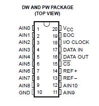
Pinout

  Connection Diagram


Specifications

Supply voltage range, VCC (see Note 1) . . . . . . . . . . . . . . . . . . . . . . . . . . . . . . . . . . . . . . . . . . . . . . . . . . . 0.5 V to 6.5 V
Input voltage range, VI (any input) . . . . . . . . . . . . . . . . . . . . . . . . . . . . . . . . . . . . . . . . . . . . . . . . . 0.3 V to VCC + 0.3 V
Output voltage range, VO . . . . . . . . . . . . . . . . . . . . . . . . . . . . . . . . . . . . . . . . . . . . . . . . . . . . . . 0.3 V to VCC + 0.3 V
Positive reference voltage, Vref+ . . . . . . . . . . . . . . . . . . . . . . . . . . . . . . . . . . . . . . . . .  . . . . . . . 0.3 V to VCC + 0.3 V
Negative reference voltage, Vref . . . . . . . . . . . . . . . . . . . . . . . . . . . . . . . . . . . . . . . . . . . . . . . . 0.3 V to VCC +0.3 V
Peak input current, II (any input) . . . . . . . . . . . . . . . . . . . . . . . . . . . . . . . . . . . . . . . . . . . . . . . . . . . . . . . . . . . . ±20 mA
Peak total input current (all inputs) . . . . . . . . . . . . . . . . . . . . . .  . . . . . . . . . . . . . . . . . . . . . . . . . . . . . . . . . . . . ±30 mA
Operating virtual junction temperature range, TJ . . . . . . . . . . . . . . . .  . . . . . . . . . . . . . . . . . . . . . . . . 40°C to 150°C
Operating free-air temperature range, TA: I . . . . . . . . . . . . . . . . . . . . . . . . . . . . . . . . . . . . . . . . . . . . . 40°C to 85°C
Storage temperature range, Tstg . . . . . . . . . . . . . . . . . . . . . . . . . . . . . . . . . . . . . . . . . . . . . . . . . . . . 65°C to 150°C
Lead temperature 1,6 mm (1/16 inch) from the case for 10 seconds . . . . . . . . . . . . . . . . . . . . . . . . . . . . . . . . . . 260°C
† Stresses beyond those listed under "absolute maximum ratings" may cause permanent damage to the device. These are stress ratings only, and functional operation of the device at these or any other conditions beyond those indicated under "recommended operating conditions" is not implied. Exposure to absolute-maximum-rated conditions for extended periods may affect device reliability.
NOTE 1: All voltage values are with respect to the GND terminal with REF and GND wired together (unless otherwise noted).


Description

The TLV2553 is a 12-bit, switched-capacitor, successive-approximation, analog-to-digital converter. The ADC has three control inputs [chip select (CS), the input-output clock, and the address/control input (DATAIN)], designed for communication with the serial port of a host processor or peripheral through a serial 3-state output.

In addition to the high-speed converter and versatile control capability, the TLV2553 device has an on-chip 14-channel multiplexer that can select any one of 11 inputs or any one of three internal self-test voltages using configuration register 1. The sample-and-hold function is automatic. At the end of conversion, when programmed as EOC, the pin 19 output goes high to indicate that conversion is complete. The converter incorporated in the device features differential, highimpedance reference inputs that facilitate ratiometric conversion, scaling, and isolation of analog circuitry from logic and supply noise. A switched-capacitor design allows low-error conversion over the full operating temperature range.

The TLV2553I is characterized for operation from TA = 40°C to 85°C. See available options table for package options.


Customers Who Bought This Item Also Bought

Margin,quality,low-cost products with low minimum orders. Secure your online payments with SeekIC Buyer Protection.
RF and RFID
Soldering, Desoldering, Rework Products
Prototyping Products
DE1
Semiconductor Modules
View more