TLV1549M

Features: 3.3-V Supply Operation 10-Bit-Resolution Analog-to-Digital Converter (ADC) Inherent Sample and Hold Function Total Unadjusted Error . . . ±1 LSB Max On-Chip System Clock Terminal Compatible With TLC1549 and TLC1549xApplication Report Available†CMOS TechnologyPinoutSpecificationsSup...

product image

TLV1549M Picture
SeekIC No. : 004522264 Detail

TLV1549M: Features: 3.3-V Supply Operation 10-Bit-Resolution Analog-to-Digital Converter (ADC) Inherent Sample and Hold Function Total Unadjusted Error . . . ±1 LSB Max On-Chip System Clock Terminal Compatibl...

floor Price/Ceiling Price

Part Number:
TLV1549M
Supply Ability:
5000

Price Break

  • Qty
  • 1~5000
  • Unit Price
  • Negotiable
  • Processing time
  • 15 Days
Total Cost: $ 0.00

SeekIC Buyer Protection PLUS - newly updated for 2013!

  • Escrow Protection.
  • Guaranteed refunds.
  • Secure payments.
  • Learn more >>

Month Sales

268 Transactions

Rating

evaluate  (4.8 stars)

Upload time: 2025/1/11

Payment Methods

All payment methods are secure and covered by SeekIC Buyer Protection PLUS.

Notice: When you place an order, your payment is made to SeekIC and not to your seller. SeekIC only pays the seller after confirming you have received your order. We will also never share your payment details with your seller.
Product Details

Description


Features:

 3.3-V Supply Operation
10-Bit-Resolution Analog-to-Digital Converter (ADC)
Inherent Sample and Hold Function
Total Unadjusted Error . . . ±1 LSB Max
On-Chip System Clock
Terminal Compatible With TLC1549 and TLC1549x
Application Report Available†
CMOS Technology


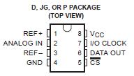
Pinout

  Connection Diagram


Specifications

Supply voltage range, VCC (see Note 1): TLV1549C . . . . . . . . . . . . . . . . . . . . . . . . . . . . . . . . . . 0.5 V to 6.5 V
                                                                 TLV1549I . . . . . . . . . . . . . . . . . . . . . . . . . . . . . . . . . . . 0.5 V to 6.5 V
                                                                 TLV1549M . . . . . . . . . . . . . . . . . . . . . . . . . . . . . . . . . . . 0.5 V to 6 V
Input voltage range, VI (any input) . . . . . . . . . . . . . . . . . . . . . . . . . . . . . . . . . . . . . . . . . . . . 0.3 V to VCC + 0.3 V
Output voltage range, VO . . . . . . . . . . . . . . . . . . . . . . . . . . . . . . . . . . . . . . . . . . . . . . . . . . . 0.3 V to VCC + 0.3 V
Positive reference voltage, Vref+ . . . . . . . . . . . . . . . . . . . . . . . . . . . . . . . . . . . . . . . . . . . . . . . . . . . . . . VCC + 0.1 V
Negative reference voltage, Vref . . . . . . . . . . . . . . . . . . . . . . . . . . . . . . . . . . . . . . . . . . . . . . . . . . . . . . . . . . 0.1 V
Peak input current (any input) . . . . . . . . . . . . . . . . . . . . . . . . . . . . . . . . . . . . . . . . . . . . . . . . . . . . . . . . . . . . ±20 mA
Peak total input current (all inputs) . . . . . . . . . . . . . . . . . . . . . . . . . . . . . . . . . . . . . . . . . . . . . . . . . . . . . . . . ±30 mA
Operating free-air temperature range, TA: TLV1549C . . . . . . . . . . . . . . . . . . . . . . . . . . . . . . . . . . . 0°C to 70°C
                                                                   TLV1549I . . . . . . . . . . . . . . . . . . . . . . . . . . . . . . . . . . 40°C to 85°C
                                                                   TLV1549M . . . . . . . . . . . . . . . . . . . . . . . . . . . . . . . . 55°C to 125°C
Storage temperature range, Tstg . . . . . . . . . . . . . . . . . . . . . . . . . . . . . . . . . . . . . . . . . . . . . . . . . . . 65°C to 150°C
Lead temperature 1,6 mm (1/16 inch) from the case for 10 seconds . . . . . . . . . . . . . . . . . . . . . . . . . . . . 260°C
† Stresses beyond those listed under "absolute maximum ratings" may cause permanent damage to the device. These are stress ratings only, and functional operation of the device at these or any other conditions beyond those indicated under "recommended operating conditions" is not implied. Exposure to absolute-maximum-rated conditions for extended periods may affect device reliability.
NOTE 1: All voltage values are with respect to ground with REF and GND wired together (unless otherwise noted).


Description

The TLV1549C, TLV1549I, and TLV1549M are 10-bit, switched-capacitor, successiveapproximation, analog-to-digital converters. The TLV1549C, TLV1549I, and TLV1549M devices have two digital inputs and a 3-state output [chip select (CS), input-output clock (I/O CLOCK), and data output (DATA OUT)] that provide a three-wire interface to the serial port of a host processor.

The sample-and-hold function is automatic. The TLV1549C, TLV1549I, and TLV1549M converter incorporated in the device features differential high-impedance reference inputs that facilitate ratiometric conversion, scaling, and isolation of analog circuitry from logic and supply noise. A switched-capacitor design allows lowerror conversion over the full operating free-air temperature range.The TLV1549C is characterized for operation from 0°C to 70°C. The TLV1549I is characterized for operation from 40°C to 85°C. The TLV1549M is characterized for operation over the full military temperature range of 55°C to 125°C.


Customers Who Bought This Item Also Bought

Margin,quality,low-cost products with low minimum orders. Secure your online payments with SeekIC Buyer Protection.
Undefined Category
Power Supplies - External/Internal (Off-Board)
Boxes, Enclosures, Racks
Optoelectronics
Audio Products
View more