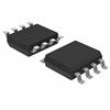
Features: Excellent Output Drive Capability
VO = ± 2.5 V Min at RL = 100 W, VCC± = ± 5 V
VO = ± 12.5 V Min at RL = 600 W, VCC± = ± 15 V
Low Supply Current . . . 280 mA Typ
Decompensated for High Slew Rate and Gain-Bandwidth Product
AVD = 0.5 Min
Slew Rate = 10 V/ms Typ
Gain-Bandwidth Product = 6.5 MHz Typ
Wide Operating Supply Voltage Range
VCC ± = ± 3.5 V to ± 18 V
High Open-Loop Gain . . . 280 V/mV Typ
Low Offset Voltage . . . 500 mV Max
Low Offset Voltage Drift With Time. . . 0.04 mV/Month Typ
Low Input Bias Current . . . 5 pA Typ
Applicationinput characteristics
The TLE2161, TLE2161A and TLE2161B are specified with a minimum and a maximum input voltage that if exceeded at either input could cause the device to malfunction.
Because of the extremely high input impedance and resulting low bias-current requirements, the TLE2161,TLE2161A, and TLE2161B are well suited for low-level signal processing; however, leakage currents on printed circuit boards and sockets can easily exceed bias-current requirements and cause degradation in system performance. It is a good practice to include guard rings around inputs (see Figure 38). These guards should be driven from a low-impedance source at the same voltage level as the common-mode input. input offset voltage nulling
The TLE2161 series offers external null pins that can further reduce the input offset voltage. The circuit in Figure 39 can be connected as shown if the feature is desired. When external nulling is not needed, the null pins may be left disconnected.SpecificationsSupply voltage, VCC + (see Note 1):19 V
Supply voltage, VCC : 19 V
Differential input voltage, VID (see Note 2) : ± 38 V
Input voltage range, VI (any input):VCC ±
Input current, II (each input):± 1 mA
Output current, IO :± 80 mA
Total current into VCC +: 80 mA
Total current out of VCC :80 mA
Duration of short-circuit current at (or below) 25°C (see Note 3) :unlimited
Continuous total power dissipation :See Dissipation Rating Table
Operating free-air temperature range, TA: C suffix : 0°C to 70°C
I suffix : 40°C to 85°C
M suffix : 55°C to 125°C
Storage temperature range, Tstg : 65°C to 150°C
Case temperature for 60 seconds: FK package :260°C
Lead temperature 1,6 mm (1/16 inch) from case for 10 seconds: D or P package: 260°C
Lead temperature 1,6 mm (1/16 inch) from case for 60seconds: JG package :300°C
† Stresses beyond those listed under "absolute maximum ratings" may cause permanent damage to the device. These are stress ratings only, and functional operation of the device at these or any other conditions beyond those indicated under "recommended operating conditions" is not implied. Exposure to absolute-maximum-rated conditions for extended periods may affect device reliability.
NOTES: 1. All voltage values, except differential voltages, are with respect to the midpoint between VCC +, and VCC .
2. Differential voltages are at IN+ with respect to IN .
3. The output may be shorted to either supply. Temperature and /or supply voltages must be limited to ensure that the maximum dissipation rating is not exceeded.
DescriptionThe TLE2161, TLE2161A, and TLE2161B are JFET-input, low-power, precision operational amplifiers manufactured using the Texas Instruments Excalibur process. Decompensated for stability with a minimum closed-loop gain of 5,
these devices combine outstanding output drive capability with low power consumption, excellent dc precision, and high gain-bandwidth product.
In addition to maintaining the traditional JFET advantages of fast slew rates and low input bias and offset currents, the Excalibur process offers outstanding parametric stability over time and temperature. This results in a TLE2161 that remains precise even with changes in temperature and over years of use.
A variety of available options includes small-outline packages and chip-carrier versions for high-density system
applications.
The C-suffix TLE2161s are characterized for operation from 0°C to 70°C. The I-suffix devices are characterized for operation from 40°C to 85°C. The M-suffix devices are characterized for operation over the full military temperature range of 55°C to 125°C.

 TLE2161 Data Sheet


