TLC7226M

Features: Four 8-Bit D/A Converters Microprocessor Compatible TTL/CMOS Compatible Single Supply Operation Possible CMOS TechnologyApplicationProcess Control Automatic Test Equipment Automatic Calibration of Large System Parameters, e.g. Gain/OffsetPinoutSpecificationsSupply voltage range, VDD: AGN...

product image

TLC7226M Picture
SeekIC No. : 004520718 Detail

TLC7226M: Features: Four 8-Bit D/A Converters Microprocessor Compatible TTL/CMOS Compatible Single Supply Operation Possible CMOS TechnologyApplicationProcess Control Automatic Test Equipment Automatic Calibr...

floor Price/Ceiling Price

Part Number:
TLC7226M
Supply Ability:
5000

Price Break

  • Qty
  • 1~5000
  • Unit Price
  • Negotiable
  • Processing time
  • 15 Days
Total Cost: $ 0.00

SeekIC Buyer Protection PLUS - newly updated for 2013!

  • Escrow Protection.
  • Guaranteed refunds.
  • Secure payments.
  • Learn more >>

Month Sales

268 Transactions

Rating

evaluate  (4.8 stars)

Upload time: 2025/1/11

Payment Methods

All payment methods are secure and covered by SeekIC Buyer Protection PLUS.

Notice: When you place an order, your payment is made to SeekIC and not to your seller. SeekIC only pays the seller after confirming you have received your order. We will also never share your payment details with your seller.
Product Details

Description


Features:

 Four 8-Bit D/A Converters
Microprocessor Compatible
TTL/CMOS Compatible
Single Supply Operation Possible
CMOS Technology


Application

 Process Control
Automatic Test Equipment
Automatic Calibration of Large System Parameters, e.g. Gain/Offset


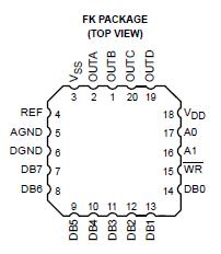
Pinout

  Connection Diagram


Specifications

Supply voltage range, VDD: AGND or DGND . . . . . . . . . . . . . . . . . . . . . . . . . . . . . . . . .  . . . . . . 0.3 V to 17 V
                                            VSS‡ . . . . . . . . . . . . . . . . . . . . . . . . . . . . . . . . . . . . . . .. . . . . . . . . 0.3 V to 24 V
Supply voltage range, VSS: AGND or DGND . . . . . . . . . . . . . . . . . . . . . . . . . . . . . . . . . . . . . . . . . 7 V to 0.3 V
Voltage range between AGND and DGND . . . . . . . . . . . . . . . . . . . . . . . . . . . . . . . . . . .. . . . . . . . 17 V to 17 V
Input voltage range, VI (to DGND) . . . . . . . . . . . . . . . . . . . . . . . . . . . . . . . . . . . . . . . . . . 0.3 V to VDD + 0.3 V
Reference voltage range: Vref (to AGND) . . . . . . . . . . . . . . . . . . . . . . . . . . . . . . . . . . . . . . . . . . . 0.3 V to VDD
                                         Vref (to VSS) . . . . . . . . . . . . . . . . . . . . . . . . . . . . . . . . . . . . . . . .. . . . . 0.3 V to 20 V
Output voltage range, VO (to AGND) (see Note 1) . . . . . . . . . . . . . . . . . . . . . . . . . . . . . . .  . . . . . . . . VSS to VDD
Continuous total power dissipation at (or below) TA = 25°C (see Note 2) . . . . . . . . . . . . . . . . . . . . . . . 500 mW
Operating free-air temperature range, TA: C suffix . . . . . . . . . . . . . . . . . . . . . . . . . . . . . . . . . . . . . 0°C to 70°C
                                                                   E suffix . . . . . . . . . . . . . . . . . . . . . . . . . . . . . . . .. . . 25°C to 85°C
                                                                   M suffix . . . . . . . . . . . . . . . . . . . . . . . . . . . . . . . . . 55°C to 125°C
Storage temperature range, Tstg . . . . . . . . . . . . . . . . . . . . . . . . . . . . . . . . . . . . . . . . . . . . . . 65°C to 150°C
Lead temperature 1,6 mm (1/16 inch) from case for 10 seconds: DW or N packages . . . . . . . . . . . . . . 260°C
Case temperature for 10 seconds: FK package . . . . . . . . . . . . . . . . . . . . . . . . . . . . . . . . . . . .  . . . . . . . . 260°C
† Stresses beyond those listed under "absolute maximum ratings" may cause permanent damage to the device. These are stress ratings only, and functional operation of the device at these or any other conditions beyond those indicated under "recommended operating conditions" is not implied. Exposure to absolute-maximum-rated conditions for extended periods may affect device reliability.
‡ The VSS terminal is connected to the substrate and must be tied to the most negative supply voltage applied to the device.
NOTES: 1. Output voltages may be shorted to AGND provided that the power dissipation of the package is not exceeded. Typically short circuit current to AGND is 60 mA.
2. For operation above TA = 75°C, derate linearly at the rate of 2 mW/°C.


Description

The TLC7226C, TLC7226I, and TLC7226M consist of four 8-bit voltage-output digital-toanalog converters (DACs) with output buffer amplifiers and interface logic on a single monolithic chip.

Separate on-chip latches are provided for each of the four DACs. Data is transferred into one of these data latches through a common 8-bit TTL/CMOS-compatible 5-V input port. Control inputs A0 and A1 determine which DAC is loaded when WR goes low. The control logic is speed compatible with most 8-bit microprocessors. Each DAC includes an output buffer amplifier capable of sourcing up to 5 mA of output current.

The TLC7226M performance is specified for input reference voltages from 2 V to VDD 4 V with dual supplies. The voltage mode configuration of the DACs allows the TLC7226 to be operated from a single power supply rail at a reference of 10 V.

The TLC7226M is fabricated in a LinBiCMOS process that has been specifically developed to allow high-speed digital logic circuits and precision analog circuits to be integrated on the same chip. The TLC7226 has a common 8-bit data bus with individual DAC latches. This provides a versatile control architecture for simple interface to microprocessors. All latch-enable signals are level triggered.

Combining four DACs, four operational amplifiers, and interface logic into either a 0.3-inch wide, 20-terminal dual-in-lineTLC7226M  (DIP) or a small 20-terminal small-outline IC (SOIC) allows a dramatic reduction in board space requirements and offers increased reliability in systems using multiple converters. The Leadless Ceramic Chip Carrier (LCCC) package provides for operation at military temperature range. The pinout is aimed at optimizing board layout with all of the analog inputs and outputs at one end of the package and all of the digital inputs at the other.


Customers Who Bought This Item Also Bought

Margin,quality,low-cost products with low minimum orders. Secure your online payments with SeekIC Buyer Protection.
Inductors, Coils, Chokes
Industrial Controls, Meters
Resistors
Transformers
View more