Features: 80 mA * 16 Bits and 120 mA * 8 Bits Drive Capability and Output Counts
5 mA to 80 mA/10 mA to 120 mA Constant Current Output Range
Constant Currency Accuracy of ±4% (Maximum Error Between Bits)
Constant Current Output Terminals
0.4 V (Output Current 0 to 40 mA)
0.7 V (Output Current 40 to 80 mA)
256 Gray Scale Display With Pulse Width Control 256 Steps
Brightness Adjustment
Output Current Adjustment for 32 Steps (Adjustment for Brightness Deviation Between LEDs)
8 Steps Brightness Control by 8 Times Speed Gray Scale Control Clock (Brightness Adjustment for Panel)
Protection
WDT Function
TSD Function
Clock Synchronized 8-Bit Parallel Input
Anode Common LED Type Applied
CMOS Input Signal Level (Schmitt-Triggered Input for All Input Terminals)
4.5 V to 5.5 V Power Supply Voltage
15 V Maximum Output Voltage
15 MHz Maximum Data Transfer Rate
4 MHz Maximum Gray Scale Clock Frequency
20°C to 85°C Operating Free-Air Temperature Range
100-Pin HTQFP Package (PD = 4.7 W, TA = 25°C)
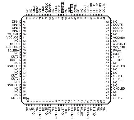
Pinout SpecificationsLogic supply voltage, VCC(LOG) . . . . . . . . . . . . . . . . 0.3 V to 7 V
Supply voltage for constant current circuit, PVCC . . . 0.3 V to 7 V
Analog supply voltage, VCC(ANA) . . . . . . . . . . . . . . . . 0.3 V to 7 V
Output current (DC), IOL(C) . . . . . . . . . . . . . . . . . . . . . . . . . .90 mA
Input voltage range 0.3 V to VCC(LOG) . . . . . . . . . . . . . . .. 0.3 V
Output voltage range,
V(OUTn), V(BOUT) and V(GSOUT) . . . . . 0.3 V to VCC(LOG) 0.3 V
Output voltage range,
V(OUTn) and V(DOWN) . . . . . . . . . . . . . . . . . . . . . .0.3 V to 0.3 V
Continuous total power dissipation at
(or below) TA = 25°C (see Note 2) . . . . . . . . . . . . . . . . . .4.7 W
Operating free air temperature range, TA . . . . . . .20°C to 85°C
Storage temperature range, Tstg . . . . . . . . . . . . 55°C to 150°C
† Stresses beyond those listed under "absolute maximum ratings" may cause permanent damage to the device. These are stress ratings only, and functional operation of the device at these or any other conditions beyond those indicated under "recommended operating conditions" is not implied. Exposure to absolute-maximum-rated conditions for extended periods may affect device reliability.
NOTES:
1. All voltage values are with respect to GNDLOG terminal.
2. For operation above 25°C free-air temperature, derate linearly at the rate of 38.2 mW/°C.DescriptionThe TLC5902 is a constant current driver that incorporates shift register, data latch, and constant current circuitry with a current value adjustable and 256 gray-scale display that uses pulse width control. The output current can be selected as maximum 80 mA with 16 bits or 120 mA with 8 bits. The current value of the constant current output is set by one external resister. After this TLC5902 is mounted on a printed-circuit board (PCB), the brightness deviation between LEDs (ICs) can be adjusted using an external data input, and the brightness control for the panel can be adjusted using the brightness adjustment circuitry. Moreover, the TLC5902 incorporates watchdog timer (WDT) circuitry, which turns the constant current output off when the scan signal is stopped during dynamic scanning operation, and thermal shutdown (TSD) circuitry, which turns constant current output off when the junction temperature exceeds the limit.

 TLC5902 Data Sheet


