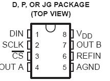
Features: Programmable Settling Time to 0.5 LSB 2.5 s or 12.5 s Typ
Two 12-Bit CMOS Voltage Output DACs in an 8-Pin Package
Simultaneous Updates for DAC A and DAC B
Single Supply Operation
3-Wire Serial Interface
High-Impedance Reference Inputs
Voltage Output Range ... 2 Times the Reference Input Voltage
Software Powerdown Mode
Internal Power-On Reset
TMS320 and SPI Compatible
Low Power Consumption:
3 mW Typ in Slow Mode,
8 mW Typ in Fast Mode
Input Data Update Rate of 1.21 MHz
Monotonic Over Temperature
Available in Q-Temp Automotive
HighRel Automotive Applications
Configuration Control / Print Support
Qualification to Automotive Standards
ApplicationBattery Powered Test Instruments
Digital Offset and Gain Adjustment
Battery Operated/Remote Industrial Controls
Machine and Motion Control Devices
Cellular TelephonesPinout Specifications
Supply voltage (VDD to AGND) . . . . . . . . . . . . . . . . . . . . . . . . . . . . . . . . . . . . . . . . . . . . . . . . . . . . . . . . . . . . . . 7 V
Digital input voltage range to AGND . . . . . . . . . . . . . . . . . . . . . . . . . . . . . . . . . . . . . . . . . . 0.3 V to VDD + 0.3 V
Reference input voltage range to AGND . . . . . . . . . . . . . . . . . . . . . . . . . . . . . . . . . . . . . . .. 0.3 V to VDD + 0.3 V
Output voltage at OUT from external source . . . . . . . . . . . . . . . . . . . . . . . . . . . . . . . . . . . . . . . . . . . . VDD + 0.3 V
Continuous current at any terminal . . . . . . . . . . . . . . . . . . . . . . . . . . . . . . . . . . . . . . . . . . . . . . . . . . . . . . ±20 mA
Operating free-air temperature range, TA: TLC5618C, TLC5618AC . . . . . . . . . . . . . . . . . . . . . . . . ...0°C to 70°C
TLC5618I, TLC5618AI . . . . . . . . . . . . . . . . . . . . . . . ........40°C to 85°C
TLC5618AQ . . . . . . . . . . . . . . . . . . . . . . . . . . . . . . . ......40°C to 125°C
TLC5618AM . . . . . . . . . . . . . . . . . . . . . . . . . . . . . . . ......55°C to 125°C
Storage temperature range, Tstg . . . . . . . . . . . . . . . . . . . . . . . . . . . . . . . . . . . . . . . . . . . . . . . . 65°C to 150°C
Lead temperature 1,6 mm (1/16 inch) from case for 10 seconds . . . . . . . . . . . . . . . . . . . . . . . . . . . . . . . ....260°C
DescriptionThe TLC5618 is a dual 12-bit voltage output digital-to-analog converter (DAC) with buffered reference inputs (high impedance). The DACs have an output voltage range that is two times the reference voltage, and the DACs are monotonic. The device is simple to use, running from a single supply of 5 V. A power-on reset function is incorporated in the device to ensure repeatable start-up conditions.
Digital control of the TLC5618 is over a 3-wire CMOS-compatible serial bus. The device re- ceives a 16-bit word for programming and producing the analog output. The digital inputs feature Schmitt triggers for high noise immunity.
Digital communication protocols include the SPITM, QSPITM, and Microwire? standards.
Two versions of the device are available. The TLC5618 does not have an internal state machine and is dependent on all external timing signals. The TLC5618A has an internal state machine that counts the number of clocks from the falling edge of CS and then updates and disables the device from accepting further data inputs. The TLC5618A is recommended for TMS320 and SPI processors, and the TLC5618 is recommended only for SPI or 3-wire serial port processors. The TLC5618A is backward-compatible and designed to work in TLC5618 designed systems.

 TLC5618 Data Sheet


