TLC5615I

Features: ·10-Bit CMOS Voltage Output DAC in an 8-Terminal Package·5-V Single Supply Operation·3-Wire Serial Interface·High-Impedance Reference Inputs·Voltage Output Range . . . 2 Times the Reference Input Voltage·Internal Power-On Reset·Low Power Consumption . . . 1.75 mW Max·Update Rate of 1.21 ...

product image

TLC5615I Picture
SeekIC No. : 004520680 Detail

TLC5615I: Features: ·10-Bit CMOS Voltage Output DAC in an 8-Terminal Package·5-V Single Supply Operation·3-Wire Serial Interface·High-Impedance Reference Inputs·Voltage Output Range . . . 2 Times the Referenc...

floor Price/Ceiling Price

Part Number:
TLC5615I
Supply Ability:
5000

Price Break

  • Qty
  • 1~5000
  • Unit Price
  • Negotiable
  • Processing time
  • 15 Days
Total Cost: $ 0.00

SeekIC Buyer Protection PLUS - newly updated for 2013!

  • Escrow Protection.
  • Guaranteed refunds.
  • Secure payments.
  • Learn more >>

Month Sales

268 Transactions

Rating

evaluate  (4.8 stars)

Upload time: 2024/5/11

Payment Methods

All payment methods are secure and covered by SeekIC Buyer Protection PLUS.

Notice: When you place an order, your payment is made to SeekIC and not to your seller. SeekIC only pays the seller after confirming you have received your order. We will also never share your payment details with your seller.
Product Details

Description


Features:

·10-Bit CMOS Voltage Output DAC in an 8-Terminal Package
·5-V Single Supply Operation
·3-Wire Serial Interface
·High-Impedance Reference Inputs
·Voltage Output Range . . . 2 Times the Reference Input Voltage
·Internal Power-On Reset
·Low Power Consumption . . . 1.75 mW Max
·Update Rate of 1.21 MHz
·Settling Time to 0.5 LSB . . . 12.5 ms Typ
·Monotonic Over Temperature
·Pin Compatible With the Maxim MAX515
·Battery-Powered Test Instruments
·Digital Offset and Gain Adjustment
·Battery Operated/Remote Industrial Controls
·Machine and Motion Control Devices
·Cellular Telephones


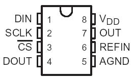
Pinout

  Connection Diagram


Specifications

Supply voltage (VDD to AGND) . . . . . . . . . . . . . . . . . . . . . . . . . . . . . . . . . 7 V
Digital input voltage range to AGND . . . . . . . . . . . . . . 0.3 V to VDD + 0.3 V
Reference input voltage range to AGND . . . . . . . . . . . 0.3 V to VDD + 0.3 V
Output voltage at OUT from external source . . . . . . . . . . . . . . . VDD + 0.3 V
Continuous current at any terminal . . . . . . . . . . . . . . . . . . . . . . . . . ±20 mA
Operating free-air temperature range, TA:TLC5615C . . . . . . ..0°C to 70°C
Operating free-air temperature range, TA:TLC5615I . . . . . 40°C to 85°C
Storage temperature range, Tstg . . . . . . . . . . . . . . . . . . .65°C to 150°C
Lead temperature 1,6 mm (1/16 inch) from case for 10 seconds . . . .260°C


Description

The TLC5615I is a 10-bit voltage output digital-to-analog converter (DAC) with a buffered reference input (high impedance). The DAC has an output voltage range that is two times the reference voltage, and the DAC is monotonic. The TLC5615I is simple to use, running from a single supply of 5 V. A power-on-reset function is incorporated to ensure repeatable start-up conditions.

Digital control of the TLC5615I is over a three-wire serial bus that is CMOS compatible and easily interfaced to industry standard microprocessor and microcontroller devices. The device receives a 16-bit data word to produce the analog output. The digital inputs feature Schmitt triggers for high noise immunity. Digital communication protocols of TLC5615I include the SPIE, QSPIE, and MicrowireE standards.

The 8-terminal small-outline D package allows digital control of analog functions in space-critical applications. The TLC5615C is characterized for operation from 0°C to 70°C. The TLC5615I is characterized for operation from 40°C to 85°C.


Customers Who Bought This Item Also Bought

Margin,quality,low-cost products with low minimum orders. Secure your online payments with SeekIC Buyer Protection.
Audio Products
Power Supplies - Board Mount
Cables, Wires - Management
Power Supplies - External/Internal (Off-Board)
View more