TLC5602C

ApplicationPhysically separate and shield external analog and digital circuitry as much as possible to reduce system noise. Use RF breadboarding or RF printed-circuit-board (PCB) techniques throughout the evaluation and production process. Since ANLG GND and DGTL GND are not connected internally, ...

product image

TLC5602C Picture
SeekIC No. : 004520676 Detail

TLC5602C: ApplicationPhysically separate and shield external analog and digital circuitry as much as possible to reduce system noise. Use RF breadboarding or RF printed-circuit-board (PCB) techniques througho...

floor Price/Ceiling Price

Part Number:
TLC5602C
Supply Ability:
5000

Price Break

  • Qty
  • 1~5000
  • Unit Price
  • Negotiable
  • Processing time
  • 15 Days
Total Cost: $ 0.00

SeekIC Buyer Protection PLUS - newly updated for 2013!

  • Escrow Protection.
  • Guaranteed refunds.
  • Secure payments.
  • Learn more >>

Month Sales

268 Transactions

Rating

evaluate  (4.8 stars)

Upload time: 2025/1/11

Payment Methods

All payment methods are secure and covered by SeekIC Buyer Protection PLUS.

Notice: When you place an order, your payment is made to SeekIC and not to your seller. SeekIC only pays the seller after confirming you have received your order. We will also never share your payment details with your seller.
Product Details

Description


Application

 Physically separate and shield external analog and digital circuitry as much as possible to reduce system noise.
Use RF breadboarding or RF printed-circuit-board (PCB) techniques throughout the evaluation and production process.
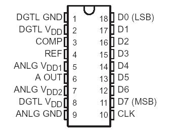
Since ANLG GND and DGTL GND are not connected internally, these terminals need to be connected externally. With breadboards, these ground lines should connect to the power-supply ground through separate leads with proper supply bypassing. A good method is to use a separate twisted pair for the analog and digital supply lines to minimize noise pickup. Use wide ground leads or a ground plane on the PCB layouts to minimize parasitic inductance and resistance. The ground plane is the better choice for noise reduction.
ANLG VDD and DGTL VDD are also separated internally, so they must connect externally. These external PCB leads should also be made as wide as possible. Place a ferrite bead or equivalent inductance in series with ANLG VDD and the decoupling capacitor as close to the device terminals as possible before the ANLG VDD and DGTL VDD leads are connected together on the board.
Decouple ANLG VDD to ANLG GND and DGTL VDD to DGTL GND with a 1-mF and 0.01-mF capacitor, respectively, as close as possible to the appropriate device terminals. A ceramic chip capacitor is recommended for the 0.01-mF capacitor.
Connect the phase compensation capacitor between COMP and ANLG GND with as short a lead-in as possible.
The no-connection (NC) terminals on the small-outline package should be connected to ANLG GND.
Shield ANLG VDD, ANLG GND, and A OUT from the high-frequency terminals CLK and D7D0. Place ANLG GND traces on both sides of the A OUT trace on the PCB.


Pinout

  Connection Diagram


Specifications

Supply voltage range, ANLG VDD, DGTL VDD . . . . . . . . . . . . . . . . . . . . . . . . . . . . . . . . . . . . . . . . .0.5 V to 7 V
Digital input voltage range, VI  . . . . . . . . . . . . . . . . . . . . . . . . . . . . . . . . . . . . . . . . . . . . . . . . . . . 0.5 V to 7 V
Analog reference voltage range, Vref . . . . . . . . . . . . . . . . . . . . . . . . . . . . . . . . . . . VDD 1.7 V to VDD + 0.5 V
Operating free-air temperature range, TA: TLC5602C . . . . . . . . . . . . . . . . . . . . . . . . . . . . . . . . . . 0°C to 70°C
TLC5602M  . . . . . . . . . . . . . . . . . . . . . . . . . . . . . . . . . . . . . . . . . . . . . . . . . . . . . . . . . . . . . . . . 55°C to 125°C
Storage temperature range, Tstg . . . . . . . . . . . . . . . . . . . . . . . . . . . . . . . . . . . . . . . . . . . . . . .65°C to 150°C
Lead temperature 1,6 mm (1/16 inch) from case for 10 seconds  . . . . . . . . . . . . . . . . . . . . . . . . . . . . . . 260°C


Description

The TLC5602C devices are low-power, ultra-high-speed video, digital-to-analog converters that use the LinEPIC™ 1-m CMOS process. The TLC5602C converts digital signals to analog signals at a sampling rate of dc to 20 MHz. Because of high-speed operation, the TLC5602C devices are suitable for digital video applications such as digital television, video processing with a computer, and radar-signal processing.

The TLC5602C is characterized for operation from 0°C to 70°C. The TLC5602M is characterized over the full military temperature range of 55°C to 125°C.


Customers Who Bought This Item Also Bought

Margin,quality,low-cost products with low minimum orders. Secure your online payments with SeekIC Buyer Protection.
Fans, Thermal Management
Motors, Solenoids, Driver Boards/Modules
LED Products
Line Protection, Backups
Batteries, Chargers, Holders
Discrete Semiconductor Products
View more