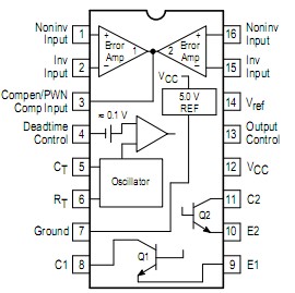
Pinout Specifications
| Rating |
Symbol |
Value |
Unit |
| Power Supply Voltage |
VCC |
42 |
V |
| Collector Output Voltage |
VC1,
VC2 |
42 |
V |
Collector Output Current
(each transistor) (Note 1) |
IC1, IC2 |
500 |
mA |
| Amplifier Input Voltage Range |
VIR |
0.3 to +42 |
V |
| Power Dissipation @ TA 45°C |
PD |
1000 |
mW |
Thermal Resistance,
JunctiontoAmbient |
RJA |
80 |
°C/W |
| Operating Junction Temperature |
TJ |
125 |
°C |
| Storage Temperature Range |
Tstg |
55 to +125 |
°C |
Operating Ambient Temperature Range
TL594ID, CN
TL594CD, IN |
TA |
0 to +70
25 to +85 |
°C |
| Derating Ambient Temperature |
TA |
45 |
°C |
NOTES: 1.Maximum thermal limits must be observed.DescriptionThe TL594 is a fixedfrequency pulse width modulation control circuit, incorporating the primary building blocks required for the control of a switching power supply. (See Figure 1.) An internallinear sawtooth oscillator is frequencyprogrammable by two external components, RT and CT. The approximate oscillator frequency is determined by:

Output pulse width modulation is accomplished by comparison of the positive sawtooth waveform across capacitor CT to either of two control signals. The NOR gates, which drive output transistors Q1 and Q2, are enabled only when the flipflop clockinput line is in its low state. This happens only during that portion of time when the sawtooth voltage is greater than the control signals. Therefore, an
increase in controlsignal amplitude causes a corresponding linear decrease of output pulse width. (Refer to the Timing Diagram shown in Figure 2.)
The TL594 control signals are external inputs that can be fed into the deadtime control, the error amplifier inputs, or the feedback input. The deadtime control comparator has an effective 120 mV input offset which limits the minimum output deadtime to approximately the first 4% of the sawtoothcycle time. This would result in a maximum duty cycle on a given output of 96% with the output control grounded, and 48% with it connected to the reference line. Additional deadtime may be imposed on the output by setting the deadtimecontrol input to a fixed voltage, ranging between 0 V to 3.3 V.
The TL594 pulse width modulator comparator provides a means for the error amplifiers to adjust the output pulse width from the maximum percent ontime, established by the deadtime control input, down to zero, as the voltage at the feedback pin varies from 0.5 V to 3.5 V. Both error amplifiers have a commonmode input range from 0.3 V to (VCC 2 V), and may be used to sense powersupply output voltage and current. The erroramplifier outputs are active high and are ORed together at the noninverting input of the pulsewidth modulator comparator. With this configuration, the amplifier that demands minimum output on time, dominates control of
the loop.
When TL594 capacitor CT is discharged, a positive pulse is generated on the output of the deadtime comparator, which clocks the pulsesteering flipflop and inhibits the output transistors, Q1 and Q2. With the outputcontrol connected to the reference line, the pulsesteering flipflop directs the modulated pulses to each of the two output transistors alternately for pushpull operation. The output frequency is equal to half that of the oscillator. Output drive can also be taken from Q1 or Q2, when singleended operation with a
maximum ontime of less than 50% is required. This is desirable when the output transformer has a ringback winding with a catch diode used for snubbing. When higher outputdrive currents are required for singleended operation, Q1 and Q2 may be connected in parallel, and the outputmode pin must be tied to ground to disable the flipflop. The output frequency will now be equal to that of the oscillator.
The TL594 has an internal 5.0 V reference capable of sourcing up to 10 mA of load current for external bias circuits. The reference has an internal accuracy of ±1.5% with a typical thermal drift of less than 50 mV over an operating temperature range of 0° to 70°C.

 TL594 Data Sheet


