Operating Supply Voltage
:
Supply Current
:
Number of Outputs
: Dual Output
Packaging
: Tube
Switching Frequency
: 300 KHz
Duty Cycle (Max)
: 45 %
Maximum Operating Temperature
: + 70 C
Minimum Operating Temperature
: 0 C
Topology
: Boost, Buck, Flyback, Forward, Full-Bridge, Half-Bridge, Push-Pull
Package / Case
: SOIC-16
Output Voltage
: 40 V
Output Current
: 200 mA
Features: · Complete PWM Power Control Circuitry
· Uncommitted Outputs for 200-mA Sink or Source Current
· Output Control Selects Single-Ended or Push-Pull Operation
· Internal Circuitry Prohibits Double Pulse at Either Output
· Variable Dead Time Provides Control Over Total Range
· Internal Regulator Provides a Stable 5-V
Reference Supply With 5% Tolerance
· Circuit Architecture Allows Easy
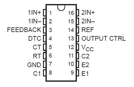
SynchronizationPinout Specifications
| |
TL494 |
UNIT |
| Supply voltage, VCC (see Note 1) |
41 |
V |
| Amplifier input voltage, VI |
VCC+0.3 |
V |
| Collector output voltage, VO |
41 |
V |
| Collector output current, IO |
250 |
mA |
| Package thermal impedance qJA (see Notes 2 and 3) |
D package |
73 |
°C |
| N package |
88 |
| NS package |
64 |
| PW package |
108 |
| Lead temperature 1,6 mm (1/16 inch) from case for 10 seconds |
D, N, or PW package |
260 |
°C |
| Storage temperature range, Tstg |
65 to 150 |
°C |
† Stresses beyond those listed under "absolute maximum ratings" may cause permanent damage to the device. These are stress ratings only, and
functional operation of the device at these or any other conditions beyond those indicated under "recommended operating conditions" is not
implied. Exposure to absolute-maximum-rated conditions for extended periods may affect device reliability.
NOTES: 1. All voltage values, except differential voltages, are with respect to the network ground terminal.
2. Maximum power dissipation is a function of TJ(max), qJA, and TA. The maximum allowable power dissipation at any allowable
ambient temperature is PD = (TJ(max) TA)/qJA. Operating at the absolute maximum TJ of 150°C can impact reliability.
3. The package thermal impedance is calculated in accordance with JESD 51, except for through-hole packages, which use a trace
length of zero.DescriptionThe TL494 incorporates all the functions required in the construction of a pulse-width-modulation (PWM) control circuit on a single chip. Designed primarily for power-supply control, this device offers the flexibility to tailor the power-supply control circuitry to a specific application.
The TL494 contains two error amplifiers, an on-chip adjustable oscillator, a dead-time control (DTC) comparator, a pulse-steering control flip-flop, a 5-V, 5%-precision regulator, and output-control circuits. The error amplifiers exhibit a common-mode voltage range from 0.3 V to VCC 2 V. The dead-time control comparator has a fixed offset that provides approximately 5% dead time. The on-chip oscillator can be bypassed by terminating RT to the reference output and providing a sawtooth input to CT, or it can drive the common circuits in synchronous multiple-rail power supplies.
The uncommitted output transistors provide either common-emitter or emitter-follower output capability. The TL494 provides for push-pull or single-ended output operation, which can be selected through the output-control function. The architecture of this device prohibits the possibility of either output being pulsed twice during push-pull operation.
The TL494C is characterized for operation from 0°C to 70°C. The TL494I is characterized for operation from 40°C to 85°C.
Parameters: | Technical/Catalog Information | TL494CD |
| Vendor | Texas Instruments |
| Category | Integrated Circuits (ICs) |
| PWM Type | Voltage Mode |
| Number of Outputs | 2 |
| Package / Case | 16-SOIC (3.9mm Width) |
| Packaging | Tube |
| Duty Cycle | 45% |
| Voltage - Supply | 7 V ~ 41 V |
| Frequency-Max | 300kHz |
| Buck | Yes |
| Boost | Yes |
| Flyback | Yes |
| Inverting | No |
| Doubler | No |
| Divider | No |
| Cuk | No |
| Isolated | No |
| Drawing Number | 296; 4040047-4; D; 16 |
| Operating Temperature | 0°C ~ 70°C |
| Lead Free Status | Lead Free |
| RoHS Status | RoHS Compliant |
| Other Names | TL494CD
TL494CD
296 1293 5 ND
29612935ND
296-1293-5
|

 TL494CD Data Sheet


