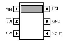
Features: Guaranteed 0.9 V Operation Very Low Quiescent Current Internal Bandgap Reference High Efficiency MOS Switching Low Output Ripple Laser-Trimmed Output Voltage Low Output Voltage Monitor Low Battery Monitor Undervoltage Lockout Regulation by Pulse Burst Modulation (PBM)Application Battery...
TK652xx: Features: Guaranteed 0.9 V Operation Very Low Quiescent Current Internal Bandgap Reference High Efficiency MOS Switching Low Output Ripple Laser-Trimmed Output Voltage Low Output Voltage Monitor Lo...
SeekIC Buyer Protection PLUS - newly updated for 2013!
268 Transactions
All payment methods are secure and covered by SeekIC Buyer Protection PLUS.
Guaranteed 0.9 V Operation
Very Low Quiescent Current
Internal Bandgap Reference
High Efficiency MOS Switching
Low Output Ripple
Laser-Trimmed Output Voltage
Low Output Voltage Monitor
Low Battery Monitor
Undervoltage Lockout
Regulation by Pulse Burst Modulation (PBM)
The TK652xx low power step-up DC-DC converter is designed for portable battery powered systems, capable of operating from a single battery cell down to 0.9 V. The TK652xx provides the power switch and the control circuit for a boost converter. The converter takes a DC input and boosts it up to a regulated 1.8, 2.1, or 2.4 V.
The output voltage is laser-trimmed. Two internal detectors monitor the output voltage and battery voltage. The Low Output Indicator (LOI) generates an active low when the battery voltage falls below 90 % of the output voltage. The Low Battery Indicator (LBI) generates an active low when the battery voltage falls below 1.1 V. These outputs can be used to notify the microprocessor or power monitor circuit of a fault condition. An internal Undervoltage Lockout (UVLO) circuit is utilized to prevent the inductor switch from remaining in the "on" mode when the battery voltage is too low to permit normal operation. Pulse Burst Modulation (PBM) is used to regulate the voltage at the VOUT pin of the IC. PBM is the process in which an oscillator signal is gated or not gated to the switch drive each period. The decision is made just before the start of each cycle and is based on comparing the output voltage to an internally-generated bandgap reference. The decision is latched, so the duty ratio is not modulated within a cycle.The average duty ratio is effectively modulated by the "bursting" and skipping of pulses which can be seen at the SW pin of the IC. Special care has been taken to achieve high reliability through the use of Oxide, double Nitride passivation. The TK652xx is available in a miniature SOT-23L-6 surface mount package.
Customized levels of accuracy in oscillator frequency and output voltage are available.